
Manual

AT75C310
109
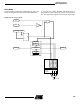
SPI Mode Register
Register Name: SP_MR
Access Type: Read/write
• MSTR: Master/Slave Mode
0 = SPI is in slave mode.
1 = SPI is in master mode.
MSTR configures the SPI interface for either master or slave mode operation.
• PS: Peripheral Select
0 = Fixed Peripheral Select.
1 = Variable Peripheral Select.
• PCSDEC: Chip Select Decode
0 = The chip selects are directly connected to a peripheral device.
1 = The four chip select lines are connected to a 4-to-16-bit decoder.
When PCSDEC equals one, up to 16 chip select signals can be generated with the four lines using an external 4-to-16-
bit decoder.
The Chip Select Register defines the characteristics of the 16 chips selected according to the following rules:
SP_CSR0 defines peripheral chip select signals 0 to 3.
SP_CSR1 defines peripheral chip select signals 4 to 7.
SP_CSR2 defines peripheral chip select signals 8 to 11.
SP_CSR3 defines peripheral chip select signals 12 to 15.
• MCK32: Clock Selection
0 = SPI master clock equals ACLK.
1 = SPI master clock equals ACLK/32.
• LLB: Local Loopback Enable
0 = Local loopback path disabled.
1 = Local loopback path enabled.
LLB controls the local loopback on the data serializer for testing in master mode only.
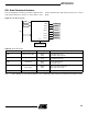
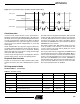
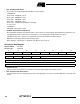
31 30 29 28 27 26 25 24
DLYBCS
23 22 21 20 19 18 17 16
–––– PCS
15 14 13 12 11 10 9 8
––––––––
76543210
LLB –––MCK32 PCSDEC PS MSTR