
User Manual


AT73C500
5
AT73C500 DSP
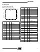
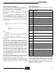
Figure 5. PLCC-44 package pin layout
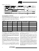
Power
Supply
Pins Pin I/O Description
VCC 35, 42 PWR Digital Supply, Positive, +5V
GND
1, 2, 6, 7,
11, 12,16,
20, 27, 30,
34
PWR Digital Supply, Negative, 0V
Digital
Inputs Pin I/O Description
CLK 44 I Clock Input
XRES 38 I Reset Input, active low
IRQ0 3 I
Interrupt Input, usually
connected to PFAIL output
of AT73C501
IRQ1 31 I
Interrupt Input, connected to
ACK Output of AT73C501
Status/
Mode
Bus Pin I/O Description
B15 17 I/O Status/Mode Bus, Bit7
B14 15 I/O Status/Mode Bus, Bit6
B13 14 I/O Status/Mode Bus, Bit5
B12 13 I/O Status/Mode Bus, Bit4
B11 29 I/O Status/Mode Bus, Bit3
B10 28 I/O Status/Mode Bus, Bit2
B9 26 I/O Status/Mode Bus, Bit1
B8 25 I/O Status/Mode Bus, Bit0
GND ADDR0
B3
GND
7 39
18
6
SOUT1
5
SOUT0
4
IRQ0 /
PFAIL
3
GND
2
GND
1
CLK
44
STROBE
43
VCC
42
NC
41
ADDR1
40
BRDY
37
XRES
38
VCC
35
RD/WR
36
SIN
33
GND
34
IRQ1 / ACK
31
SCLK
32
B11
29
GND
30
B0
8
B1
9
B2
10
GND
11
GND
12
B12
13
B13
14
B14
15
GND
16
B15
17
B4
19
GND
20
B5
21
B6
22
B7
23
N/C
24
B8
25
B9
26
GND
27
B10
28
Microprocessor
Bus Pin I/O Description
B7 23 I/O µP Bus, Bit7
B6 22 I/O µP Bus, Bit6
B5 21 I/O µP Bus, Bit5
B4 19 I/O µP Bus, Bit4
B3 18 I/O µP Bus, Bit3
B2 10 I/O µP Bus, Bit2
B1 9 I/O µP Bus, Bit1
B0 8 I/O µP Bus, Bit0
AT73C501 /
AT73C502 and
EEPROM
Interface Pin I/O Description
SOUT0 4 O
Serial Output, used as a
clock for EEPROM
SOUT1 5 O
Serial Output, used as Chip
Select (CS) for AT73C501
and as Data Input (DI) for
EEPROM
SIN 33 I
Serial Data Input, data from
AT73C501 or from EEPROM
SCLK 32 I
Serial Clock Input, bit clock
from AT73C501
Control Signals
of µP Bus and
Status/Mode
Bus Pin I/O Description
STROBE 43 O Strobe Output
BRDY 37 I
Microprocessor ready for
I/O, Active Low
ADDR1 40 O
Address Output 1, used for
µP bus
ADDR0 39 O
Address Output 0, used for
Status/ Mode bus and for
Impulse Outputs
RD/WR 36 O Read/Write Signal