
User Manual


AT73C500
4
AT73C502 Differential-Ended ADC
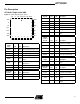
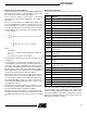
Figure 4. QFP-44 package pin layout
Power
Supply
Pins Pin I/O Description
VDA
12, 13,
29, 30
PWR
Analog Supply, Positive, +5V
VSA
10, 11,
27, 28
PWR
Analog Supply, Negative, 0V
AGND 6 PWR
Analog Ground Reference
Input
VREF 8 PWR
Reference Voltage
Output/Input
VCC 3, 4 PWR Digital Supply, Positive, +5V
VGND 32 PWR Digital Supply, Negative, 0V
Crystal
Osc
Signals Pin I/O Description
XI 43 I Crystal Oscillator Input
XO 44 O Crystal Oscillator Output
Analog
Signals Pin I/O Description
AIN2P 14 I Voltage, Channel 1, Positive
AIN2N 15 I Voltage, Channel 1, Negative
AIN4P 16 I Voltage, Channel 2, Positive
AIN4N 17 I Voltage, Channel 2, Negative
CS
BGD N/C
CLKRCLK
N/CN/CN/C
XI
RESETXO
322
133
4344
42 41 40 39 38 37 36 35 34
DATAACK
FSR
VGND
31
PD
30
VDA
29
VDA
28
VSA
27
VSA
26
SINGLE
25
AIN5N
24
AIN5P
23
AIN3N
1312 14 15 16 17 18 19 20 21 22
VCC
3
VCC
4
PFAIL
5
AGND
6
VCIN
7
VREF
8
N/C
9
VSA
10
VSA
11
AIN1NAIN6NAIN4NAIN2NVDA
AIN3PAIN1PAIN6PAIN4PAIN2PVDA
AIN6P 18 I Voltage, Channel 3, Positive
AIN6N 19 I Voltage, Channel 3, Negative
AIN1P 20 I Current, Channel 1, Positive
AIN1N 21 I Current, Channel 1, Negative
AIN3P 22 I Current, Channel 2, Positive
AIN3N 23 I Current, Channel 2, Negative
AIN5P 24 I Current, Channel 3, Positive
AIN5N 25 I Current, Channel 3, Negative
VCIN 7 I
Input to Voltage Monitoring
Block
N/C 9 I Must be left floating
Digital
Control
Signals Pin I/O Description
BGD 1 I
By-pass Control for
Reference Voltage
CS 2 I Chip Select Input
PD 31 I
Power Down Control for A/D
Modulators
N/C 33 I Connect to VGND
RESET 34 I Reset Input, Active High
SINGLE 26 I
Single / Differential selector.
· Low: Differential
· High or n/c: Single-ended
Status
Flags Pin I/O Description
PFAIL 5 O
Output of Voltage Monitoring
Block
Output
Bus
Signals Pin I/O Description
CLK 41 O Master Clock Output
CLKR 39 O Serial Bus Clock Output
DATA 35 O Serial Data Output
FSR 36 O
Output Sample Frame
Signal
ACK 37 O
Data Ready Acknowledge
Output
Analog
Signals Pin I/O Description