
User Manual


AT73C500
14
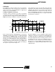
The six data packages arrive as follows:
Figure 9. Data transfer to processor in six packages
In normal mode, the Sync LS byte indicates the number of
data package which will follow (value 0...5). There are also
two special situations indicated by this byte. Value six of
Sync LS byte means that the processor is expected to sup-
ply calibration data to AT73C500. Value seven is written by
AT73C500 in case power interruption is detected and bill-
ing information needs to be transferred to microprocessor.
In this case the processor knows that both packages 3 and
4 will follow one after each other as shown in Figure 10.
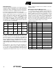
Table 5. Package 4
Byte Data Order Meaning
1 Sync LS Single byte Synchronization
2 Sync MS Single byte Synchronization
3 Mode Single byte Mode information
4 Status Single byte Status information
5 REG15 (LS+2) byte
Reactive energy,
capacitive load
6 REG15 MS byte
Reactive energy,
capacitive load
7 REG15 LS byte
Reactive energy,
capacitive load
8 REG15 (LS+1) byte
Reactive energy,
capacitive load
9 REG16 (LS+2) byte Counter
10 REG16 MS byte Counter
11 REG16 LS byte Counter
12 REG16 (LS+1) byte Counter
13 REG17 LS byte Frequency
14 REG17 MS byte Frequency
15 REG18 LS byte Reserved
16 REG18 MS byte Reserved
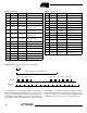
Table 6. Package 5
Byte Data Order Meaning
1 Sync LS Single byte Synchronization
2 Sync MS Single byte Synchronization
3 Mode Single byte Mode information
4 Status Single byte Status information
5 REG19 LS byte Voltage, phase 1
6 REG19 MS byte Voltage, phase 1
7 REG20 LS byte Voltage, phase 2
8 REG20 MS byte Voltage, phase 2
9 REG21 LS byte Voltage, phase 3
10 REG21 MS byte Voltage, phase 3
11 REG22 LS byte Current, phase 1
12 REG22 MS byte Current, phase 1
13 REG23 LS byte Current, phase 2
14 REG23 MS byte Current, phase 2
15 REG24 LS byte Current, phase 3
16 REG24 MS byte Current, phase 3
1234567891012345
200ms = 655360 clocks @ 3.2768 MHz
20 ms
Pack
0
Pack
1
Pack
2
Pack
3
Pack
4
Pack
5
Pack
0
Pack
1
Pack
2
Pack
3
DATRDY
LINE PERIOD