
Manual

6
AT49BV512
1026E–FLASH–06/02
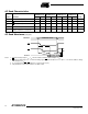
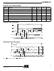
AC Read Waveforms
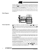
(1)(2)(3)(4)
Notes: 1. CE may be delayed up to t
ACC
-t
CE
after the address transition without impact on t
ACC
.
2. OE
may be delayed up to t
CE
-t
OE
after the falling edge of CE without impact on t
CE
or by t
ACC
-t
OE
after an address change
without impact on t
ACC
.
3. t
DF
is specified from OE or CE whichever occurs first (CL - 5 pF).
4. This parameter is characterized and is not 100% tested.
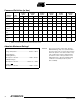
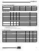
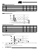
AC Read Characteristics
Symbol Parameter
AT49BV512-70 AT49BV512-90 AT49BV512-12 AT49BV512-15
UnitsMin Max Min Max Min Max Min Max
t
ACC
Address to Output Delay 70 90 120 150 ns
t
CE
(1)
CE to Output Delay 70 90 120 150 ns
t
OE
(2)
OE to Output Delay 0 35 40 50 0 70 ns
t
DF
(3, 4)
CE or OE to Output Float 0 25 0 25 0 30 0 40 ns
t
OH
Output Hold from OE,CEor
Address, whichever occurred first
0000ns
ADDRESS
CE
OUTPUT
OE
OUTPUT VALID
tACC
ADDRESS VALID
HIGH Z
tDF
tCE
tOH