
User Manual

17
AT45DB642
1638F–DFLSH–09/02
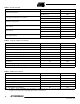
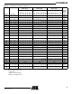
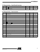
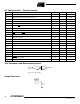
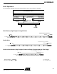
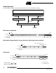
AC Waveforms Two different timing diagrams are shown below. Waveform 1 shows the SCK/CLK signal
being low when CS
makes a high-to-low transition, and Waveform 2 shows the SCK/CLK sig-
nal being high when CS
makes a high-to-low transition. Both waveforms show valid timing
diagrams. The setup and hold times for the input signals (SI or I/O7-I/O0) are referenced to the
low-to-high transition on the SCK/CLK signal.
Waveform 1 shows timing that is also compatible with SPI Mode 0, and Waveform 2 shows
timing that is compatible with SPI Mode 3.
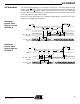
Waveform 1 –
Inactive Clock
Polarity Low and
SPI Mode 0
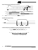
Waveform 2 –
Inactive Clock
Polarity High and
SPI Mode 3
CS
SCK/CLK
SI or I/O7 - I/O0
(INPUT)
SO or I/O7 - I/O0
(OUTPUT)
tCSS
VALID IN
tHtSU
tWH tWL tCSH
tCS
tV
HIGH IMPEDANCE
VALID OUT
tHO tDIS
HIGH IMPEDANCE
CS
SCK/CLK
SO or I/O7 - I/O0
(OUTPUT)
tCSS
VALID IN
tHtSU
tWL tWH tCSH
tCS
tV
HIGH Z
VALID OUT
tHO tDIS
HIGH IMPEDANCE
SI or I/O7 - I/O0
(INPUT)