
Owner's manual

56
Adesto AT45DB161E [DATASHEET]
8782D–DFLASH–11/2012
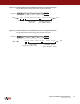
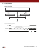
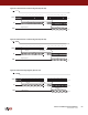
Figure 24-3. Main Memory Page to Buffer Transfer
Data From the selected Flash Page is read into either SRAM Buffer
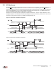
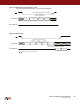
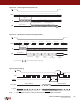
Figure 24-4. Buffer Read
CS
SI (Input)
CMD PA11-6 PA5-0, XX XXXX XX
Starts Reading Page Data into Buffer
Binary Page Size
A20-A9 + 9 Dummy Bits
SO (Output)
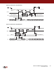
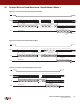
CS
SI (Input)
SO (Output)
n
CMD X X... X, BFA9-8 BFA7-0 X
Address for Binary Page Size
A20-A16 A15-A8 A7-A0
n n + 1
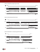
No Dummy Byte (opcodes D1H and D3H)
1 Dummy Byte (opcodes D4H and D6H)
Each transition represents eight bits