
Owner's manual


26
Adesto AT45DB161E [DATASHEET]
8782D–DFLASH–11/2012
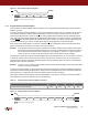
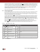
Figure 8-4. Program Security Register
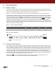
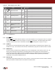
8.2.2 Reading the Security Register
To read the Security Register, an opcode of 77h and three dummy bytes must be clocked into the device. After the last
dummy bit has been clocked in, the contents of the Security Register can be clocked out on the SO pin. After the last
byte of the Security Register has been read, additional pulses on the SCK pin will result in undefined data being output
on the SO pin.
Deasserting the
CS pin will terminate the Read Security Register operation and put the SO pin into a high-impedance
state.
Figure 8-5. Read Security Register
Data
n
9Bh 00h 00h 00h
Data
n + 1
Data
n + x
CS
SI
Each transition represents eight bits
77h XX XX XX
Data
n
Data
n + 1
CS
Data
n + x
SI
SO
Each transition represents eight bits