
User Manual


5
AT45DB161B
2224E–DFLSH–10/02
loaded into the device. After the last bit of the opcode is shifted in, the eight bits of the
status regis ter, st arting with the MSB (bit 7), wil l be shift ed out on the SO pin during the
next eight clock cy cles. The five most significant bits of the status register will conta in
device information, while the remaining three least-significant bits are reserved for future
use and will have und efined value s. After bit 0 of the status regis ter has been shifte d
out, the sequence will repeat itself (as long as CS
remains low and SCK is being tog-
gled) starting again with bit 7. The data in the status register is constantly updated, so
each repeating sequence will output new data.
Ready/Busy status is indicated using bit 7 of the status register. If bit 7 is a 1, then the
device is not busy and is ready to accept the next command. If bit 7 is a 0, then the
device is in a busy state. The user can continuously poll bit 7 of the status register by
stopping S CK at a low lev el on ce bi t 7 has been ou tput . Th e status o f b it 7 wi ll continue
to be output on the SO pin, and once the device is no longer busy, the state of SO will
change from 0 to 1. There ar e eight operations which can cause the device to be in a
busy state: Main Memory Page to Buffer Transfer, Main Memory Page to Buffer Com-
pare, B uffer to Ma in Me mory P age P rogram with Built- in E rase, B uffer to M ain M emory
Page Program without Built-in Erase, Page Erase, Block Erase, Main Memory Page
Program, and Auto Page Rewrite.
The result of the most recent Main Memory Page to Buffer Compare operation is indi-
cated using bit 6 of the status register. If bit 6 is a 0, then the data in the main memory
page matches the data in the buffer. If bit 6 is a 1, then at least one bit of the data in the
main memory page does not match the data in the buffer.
The device density is indicated using bits 5, 4, 3 and 2 of the status register. For the
AT45DB161B, the four bits are 1, 0, 1 and 1. The decimal value of these four binary bits
does not equate to the device density; the fou r bits represent a combi national code
relating to di fferin g den sities of S erial DataFl ash dev ices , allowi ng a total of s ixteen dif-
ferent density configurations.
Program and Erase
Commands
BUFFER WRITE: Data can be shifted i n from the S I pin into ei ther buffe r 1 or buffe r 2.
To load data into either buffer, an 8-bit opcode, 84H for buffer 1 or 87H for buffer 2, must
be follo wed by 14 don’t care bits and ten ad dress bi ts (BFA9 - BFA 0). The te n addre ss
bits sp ecify the fi rst byte i n the buffer to be writte n. The dat a is entered fo llowin g the
address bits. If the end of the data buffer is reached, the device will wrap around back to
the beginni ng of the bu ffer. Dat a will cont inue to be loaded into th e buffer until a low- to-
high transition is detected on the CS
pin.
BUFFER TO MAIN ME MORY PAG E PROGRAM WI TH BUILT-IN E RASE: Data written
into either buffer 1 or buffer 2 can be programmed into the main memory. To start the
operati on, an 8-bit opc ode , 83H fo r buffe r 1 or 86H for bu ffer 2, m us t be fol lo wed by the
two reserved bits, 12 address bits (PA11 - PA0) that specify the page in the main
memory to be written, and ten additional don’t care bits. When a low-to-high transition
occurs on the CS
pin, the part will first erase the selected page in main memory to all 1s
and then program the data stored in the buffer into the specified page in the main mem-
ory. Both the erase and the programming of the page are internally self-timed and
should take place in a maximum time of t
EP
. During this time, the status register will indi-
cate that the part is busy.
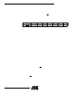
Status Register Format
Bit 7 Bit 6 Bit 5 Bit 4 Bit 3 Bit 2 Bit 1 Bit 0
RDY/BUSY COMP1011XX