
User Manual


3
AT45DB161B
2224E–DFLSH–10/02
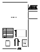
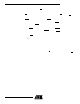
Memory Architecture Diagram
Device Operation The device operation is controlled by instructions from the host processor. The list of
instructions and their associated opcodes are contained in Tables 1 through 4. A valid
instr uction starts wit h the falling ed ge of CS
follo wed by the app ropriate 8 -bit opc ode
and the desired buffer or main memory address location. While the CS
pin is low, tog-
gling the SCK pin controls the loading of the opc ode and the desired buffer or main
memo ry address loca tion through the SI (serial input) pin . All in structi ons, address es
and data are transferred with the most significant bit (MSB) first.
Buffe r addressin g is referen ced in the dat asheet us ing the termin ology BFA 9 - B FA0 to
denote the ten address bits required to designate a byte address within a buffer. Main
memory addressing is referenced using the terminology PA11 - PA0 and BA 9 - BA0
where PA11 - PA0 denotes the 12 address bits requi red to designate a pag e address
and BA9 - BA0 denotes the ten address bits required to designate a byte address within
the page.
Read Commands By speci fying the appr opriate opcode, da ta can be read from the main memory or fro m
either one of the two data buffers. The DataFlash supports two categories of read
modes in rela tion to th e SCK s ignal. T he dif ferences betwee n the mod es ar e in res pect
to the inac tive s tate of the SCK si gnal as wel l as whic h cloc k cycle da ta will begin to be
output. T he two categories, which are comprised of four modes total, are defined as
Inactive Clock Polarity Low or Inactive Clock Polarity High and SPI Mode 0 or SPI
Mode 3. A separate opcode (refer to Table 1 on page 10 for a complete list) is used to
select which category will be used for reading. Please refer to the “Detailed Bit-level
Read Tim ing” dia grams in this datas heet for details on the clock cycle se quences for
each mode.
CONTINUOUS ARRAY READ: By s upplying an initial starting address for the main
memory array, the Continuous Array Read command can b e utilized to sequentially
read a conti nuous stream of data from the de vice by simp ly provi ding a cl ock sig nal; no
additional addressing information or control signals need to be provided. The DataFlash
incorporates an internal address counter that will automatically increment on every clock
Block = 4224 bytes
(4K + 128)
8 Pages
BLOCK 0
BLOCK 1
BLOCK 30
BLOCK 31
BLOCK 32
BLOCK 33
BLOCK 510
BLOCK 511
BLOCK 62
BLOCK 63
BLOCK 64
BLOCK 65
BLOCK 66
BLOCK 509
Page = 528 bytes
(512 + 16)
PAGE 0
PAGE 1
PAGE 6
PAGE 7
PAGE 8
PAGE 9
PAGE 4094
PAGE 4095
BLOCK 0
PAGE 14
PAGE 15
PAGE 16
PAGE 17
PAGE 18
PAGE 4093
BLOCK 1
BLOCK ARCHITECTURE PAGE ARCHITECTURE
SECTOR 0
SECTOR 1SECTOR 2
SECTOR 0 = 8 Pages
4,224 bytes (4K + 128)
SECTOR 1 = 248 Pages
130,944 bytes (124K + 3,968)
SECTOR ARCHITECTURE
SECTOR 16 = 256 Pages
135,168 bytes (128K + 4K)
SECTOR 2 = 256 Pages
135,168 bytes (128K + 4K)
SECTOR 3 = 256 Pages
135,168 bytes (128K + 4K)