
User Manual


2
AT45DB161B
2224E–DFLSH–10/02
stream. EEPROM emulation (bit or byte alterability) is easily handle d with a self-
contai ned th ree step Read -Modi fy-Writ e operation .Unlik e conventi onal Flas h memori es
that are acc essed randomly with mu ltiple address lines and a parallel inter face, the
DataFla sh uses a SPI ser ial interface to se quentially ac cess its data. Data Flash s up-
ports SPI mode 0 and m ode 3. The simple serial interface facilitates hardware layout,
increases system reliability, minimizes switching noise, and reduces package size and
active pin count. The device i s optimized for use in many commercial and industria l
applications where high density, low pin count, low voltage, and low power are essential.
The device operates at clock frequencies up to 20 MHz with a typical active read current
consumption of 4 mA.
To allow for simple in-system reprogrammability, the AT45DB161B does not require
high input voltages for programming. The device oper ates from a single power supply,
2.5V to 3.6V or 2.7V to 3.6V, for both the program and read operations. The
AT45DB161B is enabled through the chip select pin (CS
) and accessed via a three-wire
interface consisting of the Serial Input (SI), Serial Output (SO), and the Serial Clock
(SCK).
All programming cycles are self-timed, and no separate erase cycle is required before
programming.
When the device is shipped from Atmel, the most significant page of the memory array
may not be erased. In other words, the contents of the last page may not be filled with
FFH.
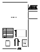
Block Diag ram
Memory Array
To provide optimal flexibility, the memory array of the AT45DB161B is divided into three
levels of granularity comprising of sectors, blocks, and pages. The Memory Architecture
Diagra m illu strates the b reakdown of eac h leve l and details the nu mber o f pages per
sector and block. All program operations to the DataFlash occur on a page-by-page
basis ; howe ver, the optiona l erase opera tions can be pe rformed at the blo ck or page
level.
FLASH MEMORY ARRAY
PAGE (528 BYTES)
BUFFER 2 (528 BYTES)BUFFER 1 (528 BYTES)
I/O INTERFACE
SCK
CS
RESET
VCC
GND
RDY/BUSY
WP
SOSI