
User guide

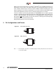
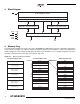


Table Of Contents
- Features
- 1. Description
- 2. Pin Configurations and Pinouts
- 3. Block Diagram
- 4. Memory Array
- 5. Device Operation
- 6. Read Commands
- 7. Program and Erase Commands
- 8. Sector Protection
- 9. Hardware Controlled Protection
- 10. Security Features
- 11. Additional Commands
- 12. Deep Power-down
- 13. “Power of 2” Binary Page Size Option
- 14. Manufacturer and Device ID Read
- 15. Command Tables
- 16. Power-on/Reset State
- 17. System Considerations
- 18. Electrical Specifications
- 19. Input Test Waveforms and Measurement Levels
- 20. Output Test Load
- 21. AC Waveforms
- 21.1 Waveform 1 – SPI Mode 0 Compatible (for Frequencies up to 66MHz)
- 21.2 Waveform 2 – SPI Mode 3 Compatible (for Frequencies up to 66MHz)
- 21.3 Waveform 3 – RapidS Mode 0 (FMAX = 66MHz)
- 21.4 Waveform 4 – RapidS Mode 3 (FMAX = 66MHz)
- 21.5 Utilizing the RapidS Function
- 21.6 Reset Timing
- 21.7 Command Sequence for Read/Write Operations for Page Size 256-Bytes (Except Status Register Read, Manufacturer and Device ID Read)
- 21.8 Command Sequence for Read/Write Operations for Page Size 264-Bytes (Except Status Register Read, Manufacturer and Device ID Read)
- 22. Write Operations
- 23. Read Operations
- 24. Detailed Bit-level Read Waveform – RapidS Serial Interface Mode 0/Mode 3
- 24.1 Continuous Array Read (Legacy Opcode E8H)
- 24.2 Continuous Array Read (Opcode 0BH)
- 24.3 Continuous Array Read (Low Frequency: Opcode 03H)
- 24.4 Main Memory Page Read (Opcode: D2H)
- 24.5 Buffer Read (Opcode D4H or D6H)
- 24.6 Buffer Read (Low Frequency: Opcode D1H or D3H)
- 24.7 Read Sector Protection Register (Opcode 32H)
- 24.8 Read Sector Lockdown Register (Opcode 35H)
- 24.9 Read Security Register (Opcode 77H)
- 24.10 Status Register Read (Opcode D7H)
- 24.11 Manufacturer and Device Read (Opcode 9FH)
- 25. Auto Page Rewrite Flowchart
- 26. Ordering Information
- 27. Packaging Information
- 28. Revision History
- 29. Errata

7
3596N–DFLASH–11/2012
AT45DB081D
during the page boundary crossover (the crossover from the end of one page to the beginning of
the next page). When the last bit in the main memory array has been read, the device will con-
tinue reading back at the beginning of the first page of memory. As with crossing over page
boundaries, no delays will be incurred when wrapping around from the end of the array to the
beginning of the array. A low-to-high transition on the CS pin will terminate the read operation
and tri-state the output pin (SO). The Continuous Array Read bypasses both data buffers and
leaves the contents of the buffers unchanged.
6.4 Main Memory Page Read
A main memory page read allows the user to read data directly from any one of the 4,096 pages
in the main memory, bypassing both of the data buffers and leaving the contents of the buffers
unchanged. To start a page read from the DataFlash standard page size (264-bytes), an opcode
of D2H must be clocked into the device followed by three address bytes (which comprise the
24-bit page and byte address sequence) and four don’t care bytes. The first 12 bits (PA11 -
PA0) of the 21-bit address sequence specify the page in main memory to be read, and the last
nine bits (BA8 - BA0) of the 21-bit address sequence specify the starting byte address within
that page. To start a page read from the binary page size (256-bytes), the opcode D2H must be
clocked into the device followed by three address bytes and four don’t care bytes. The first 12
bits (A19 - A8) of the 20-bits sequence specify which page of the main memory array to read,
and the last eight bits (A7 - A0) of the 20-bits address sequence specify the starting byte
address within the page. The don’t care bytes that follow the address bytes are sent to initialize
the read operation. Following the don’t care bytes, additional pulses on SCK result in data being
output on the SO (serial output) pin. The
CS pin must remain low during the loading of the
opcode, the address bytes, the don’t care bytes, and the reading of data. When the end of a
page in main memory is reached, the device will continue reading back at the beginning of the
same page. A low-to-high transition on the CS pin will terminate the read operation and tri-state
the output pin (SO). The maximum SCK frequency allowable for the Main Memory Page Read is
defined by the f
SCK
specification. The Main Memory Page Read bypasses both data buffers and
leaves the contents of the buffers unchanged.
6.5 Buffer Read
The SRAM data buffers can be accessed independently from the main memory array, and utiliz-
ing the Buffer Read Command allows data to be sequentially read directly from the buffers. Four
opcodes, D4H or D1H for buffer 1 and D6H or D3H for buffer 2 can be used for the Buffer Read
Command. The use of each opcode depends on the maximum SCK frequency that will be used
to read data from the buffer. The D4H and D6H opcode can be used at any SCK frequency up to
the maximum specified by f
CAR1
. The D1H and D3H opcode can be used for lower frequency
read operations up to the maximum specified by f
CAR2
.
To perform a buffer read from the standard DataFlash buffer (264-bytes), the opcode must be
clocked into the device followed by three address bytes comprised of 15 don’t care bits and
nine buffer address bits (BFA8 - BFA0). To perform a buffer read from the binary buffer (256-
bytes), the opcode must be clocked into the device followed by three address bytes comprised
of 16 don’t care bits and eight buffer address bits (BFA7 - BFA0). Following the address bytes,
one don’t care byte must be clocked in to initialize the read operation. The CS pin must remain
low during the loading of the opcode, the address bytes, the don’t care bytes, and the reading of
data. When the end of a buffer is reached, the device will continue reading back at the beginning
of the buffer. A low-to-high transition on the CS pin will terminate the read operation and tri-state
the output pin (SO).