
User guide
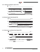
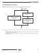
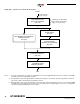
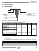
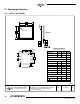
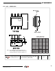
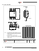
Table Of Contents
- Features
- 1. Description
- 2. Pin Configurations and Pinouts
- 3. Block Diagram
- 4. Memory Array
- 5. Device Operation
- 6. Read Commands
- 7. Program and Erase Commands
- 8. Sector Protection
- 9. Hardware Controlled Protection
- 10. Security Features
- 11. Additional Commands
- 12. Deep Power-down
- 13. “Power of 2” Binary Page Size Option
- 14. Manufacturer and Device ID Read
- 15. Command Tables
- 16. Power-on/Reset State
- 17. System Considerations
- 18. Electrical Specifications
- 19. Input Test Waveforms and Measurement Levels
- 20. Output Test Load
- 21. AC Waveforms
- 21.1 Waveform 1 – SPI Mode 0 Compatible (for Frequencies up to 66MHz)
- 21.2 Waveform 2 – SPI Mode 3 Compatible (for Frequencies up to 66MHz)
- 21.3 Waveform 3 – RapidS Mode 0 (FMAX = 66MHz)
- 21.4 Waveform 4 – RapidS Mode 3 (FMAX = 66MHz)
- 21.5 Utilizing the RapidS Function
- 21.6 Reset Timing
- 21.7 Command Sequence for Read/Write Operations for Page Size 256-Bytes (Except Status Register Read, Manufacturer and Device ID Read)
- 21.8 Command Sequence for Read/Write Operations for Page Size 264-Bytes (Except Status Register Read, Manufacturer and Device ID Read)
- 22. Write Operations
- 23. Read Operations
- 24. Detailed Bit-level Read Waveform – RapidS Serial Interface Mode 0/Mode 3
- 24.1 Continuous Array Read (Legacy Opcode E8H)
- 24.2 Continuous Array Read (Opcode 0BH)
- 24.3 Continuous Array Read (Low Frequency: Opcode 03H)
- 24.4 Main Memory Page Read (Opcode: D2H)
- 24.5 Buffer Read (Opcode D4H or D6H)
- 24.6 Buffer Read (Low Frequency: Opcode D1H or D3H)
- 24.7 Read Sector Protection Register (Opcode 32H)
- 24.8 Read Sector Lockdown Register (Opcode 35H)
- 24.9 Read Security Register (Opcode 77H)
- 24.10 Status Register Read (Opcode D7H)
- 24.11 Manufacturer and Device Read (Opcode 9FH)
- 25. Auto Page Rewrite Flowchart
- 26. Ordering Information
- 27. Packaging Information
- 28. Revision History
- 29. Errata

Corporate Office
California | USA
Adesto Headquarters
1250 Borregas Avenue
Sunnyvale, CA 94089
Phone: (+1) 408.400.0578
Email: contact@adestotech.com
© 2012 Adesto Technologies. All rights reserved. / Rev.: 3596N–DFLASH–11/2012
Disclaimer: The information in this document is provided in connection with Adesto products. No license, express or implied, by estoppel or otherwise, to any intellectual property right is granted by this
document or in connection with the sale of Adesto products. EXCEPT AS SET FORTH IN THE ADESTO TERMS AND CONDITIONS OF SALES LOCATED ON THE ADESTO WEBSITE, ADESTO
ASSUMES NO LIABILITY WHATSOEVER AND DISCLAIMS ANY EXPRESS, IMPLIED OR STATUTORY WARRANTY RELATING TO ITS PRODUCTS INCLUDING, BUT NOT LIMITED TO, THE
IMPLIED WARRANTY OF MERCHANTABILITY, FITNESS FOR A PARTICULAR PURPOSE, OR NON-INFRINGEMENT. IN NO EVENT SHALL ADESTO BE LIABLE FOR ANY DIRECT, INDIRECT,
CONSEQUENTIAL, PUNITIVE, SPECIAL OR INCIDENTAL DAMAGES (INCLUDING, WITHOUT LIMITATION, DAMAGES FOR LOSS AND PROFITS, BUSINESS INTERRUPTION, OR LOSS OF
INFORMATION) ARISING OUT OF THE USE OR INABILITY TO USE THIS DOCUMENT, EVEN IF ADESTO HAS BEEN ADVISED OF THE POSSIBILITY OF SUCH DAMAGES. Adesto makes no
representations or warranties with respect to the accuracy or completeness of the contents of this document and reserves the right to make changes to specifications and products descriptions at any time
without notice. Adesto does not make any commitment to update the information contained herein. Unless specifically provided otherwise, Adesto products are not suitable for, and shall not be used in,
automotive applications. Adesto products are not intended, authorized, or warranted for use as components in applications intended to support or sustain life.
Adesto
®
, the Adesto logo, CBRAM
®
, and DataFlash
®
are registered trademarks or trademarks of Adesto Technologies. All other marks are the property of their respective
owners.