
User guide
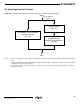
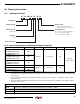
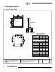
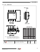
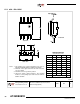

Table Of Contents
- Features
- 1. Description
- 2. Pin Configurations and Pinouts
- 3. Block Diagram
- 4. Memory Array
- 5. Device Operation
- 6. Read Commands
- 7. Program and Erase Commands
- 8. Sector Protection
- 9. Hardware Controlled Protection
- 10. Security Features
- 11. Additional Commands
- 12. Deep Power-down
- 13. “Power of 2” Binary Page Size Option
- 14. Manufacturer and Device ID Read
- 15. Command Tables
- 16. Power-on/Reset State
- 17. System Considerations
- 18. Electrical Specifications
- 19. Input Test Waveforms and Measurement Levels
- 20. Output Test Load
- 21. AC Waveforms
- 21.1 Waveform 1 – SPI Mode 0 Compatible (for Frequencies up to 66MHz)
- 21.2 Waveform 2 – SPI Mode 3 Compatible (for Frequencies up to 66MHz)
- 21.3 Waveform 3 – RapidS Mode 0 (FMAX = 66MHz)
- 21.4 Waveform 4 – RapidS Mode 3 (FMAX = 66MHz)
- 21.5 Utilizing the RapidS Function
- 21.6 Reset Timing
- 21.7 Command Sequence for Read/Write Operations for Page Size 256-Bytes (Except Status Register Read, Manufacturer and Device ID Read)
- 21.8 Command Sequence for Read/Write Operations for Page Size 264-Bytes (Except Status Register Read, Manufacturer and Device ID Read)
- 22. Write Operations
- 23. Read Operations
- 24. Detailed Bit-level Read Waveform – RapidS Serial Interface Mode 0/Mode 3
- 24.1 Continuous Array Read (Legacy Opcode E8H)
- 24.2 Continuous Array Read (Opcode 0BH)
- 24.3 Continuous Array Read (Low Frequency: Opcode 03H)
- 24.4 Main Memory Page Read (Opcode: D2H)
- 24.5 Buffer Read (Opcode D4H or D6H)
- 24.6 Buffer Read (Low Frequency: Opcode D1H or D3H)
- 24.7 Read Sector Protection Register (Opcode 32H)
- 24.8 Read Sector Lockdown Register (Opcode 35H)
- 24.9 Read Security Register (Opcode 77H)
- 24.10 Status Register Read (Opcode D7H)
- 24.11 Manufacturer and Device Read (Opcode 9FH)
- 25. Auto Page Rewrite Flowchart
- 26. Ordering Information
- 27. Packaging Information
- 28. Revision History
- 29. Errata
51
3596N–DFLASH–11/2012
AT45DB081D
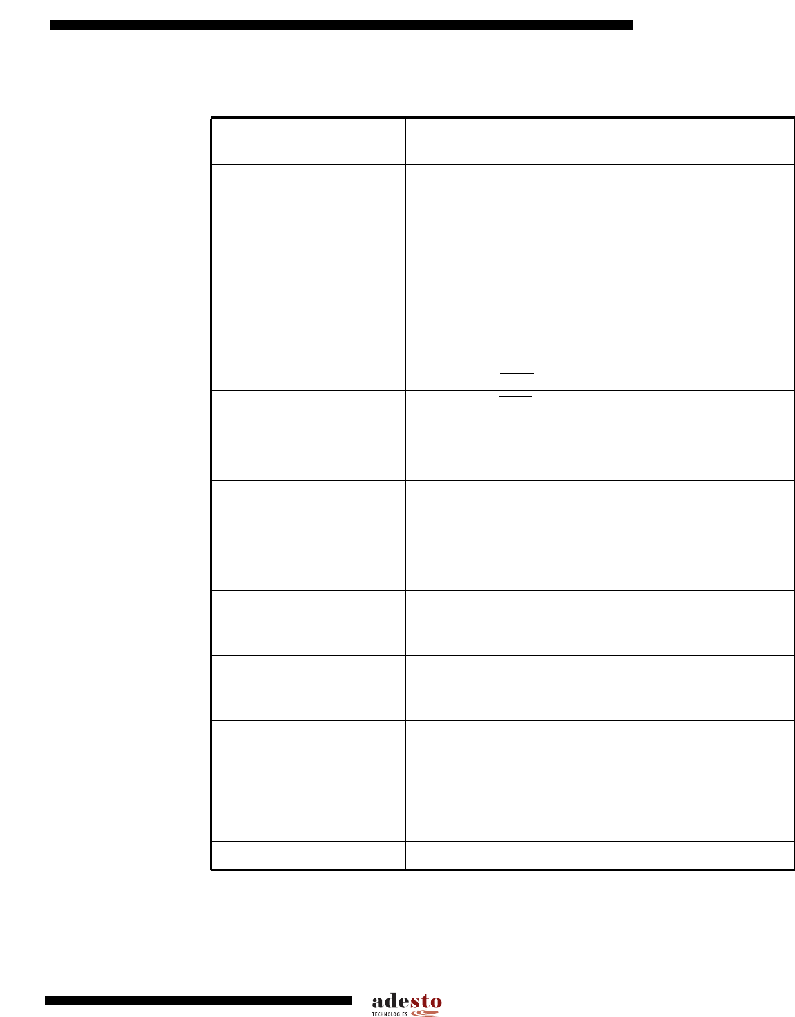
28. Revision History
Revision Level – Release Date History
A – November 2005 Initial Release
B – March 2006
Added Preliminary.
Added text, in “Programming the Configuration Register”, to indicate
that power cycling is required to switch to “power of 2” page size
after the opcode enable has been executed.
Added “Legacy Commands” table.
C – July 2006
Corrected PA3 in opcode 50h for addressing sequence with
standard page size. Corrected Chip Erase opcode from 7CH to
C7H. Clarified the commands B and C usage for operation mode.
D – November 2006
Removed Preliminary.
Added errata regarding Chip Erase.
Changed various timing parameters under Table 18-4.
E – February 2007 Removed RDY/
BUSY pin references.
F – August 2007
Removed SER/
BYTE statement from SI and SO pin descriptions in
Table 2-1.
Added additional text to “power of 2” binary page size option.
Changed t
VSCL
from 50µs to 70µs.
Changed t
RDPD
from 30µs to 35µs.
G – January 2008
Added additional text, in “power of 2” binary page size option, to
indicate that the address format is changed for devices with page
size set to 256-bytes.
Corrected typographical error to indicate that Figure 13-1 indicates
Program Configuration Register.
H – January 2008 Removed DataFlash card pinout.
I – April 2008
Added part number ordering code details for suffixes SL954/955
Added ordering code details.
J – February 2009 Changed t
DIS
(Typ and Max) to 27ns and 35ns, respectively.
K – March 2009
Changed Deep Power-Down Current values
- Increased typical value from 5µA to 15µA.
- Increased maximum value from 15µA to25 µA.
L – April 2009
Updated Absolute Maximum Ratings
Removed Chip Erase Errata
M – May 2010
Changed t
SE
(Typ) 1.6 to 0.7 and (Max) 5 to 1.3
Changed t
CE
(Typ) TBD to 7 and (Max) TBD to 22
Changed from 10,000 to 20,000 cumulative page erase/program
operations and added the contact statement in section 11.3.
N – November 2010 Update to Adesto.