
User guide
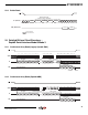
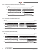
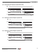
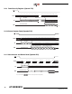
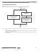
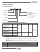
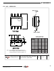
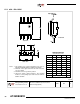
Table Of Contents
- Features
- 1. Description
- 2. Pin Configurations and Pinouts
- 3. Block Diagram
- 4. Memory Array
- 5. Device Operation
- 6. Read Commands
- 7. Program and Erase Commands
- 8. Sector Protection
- 9. Hardware Controlled Protection
- 10. Security Features
- 11. Additional Commands
- 12. Deep Power-down
- 13. “Power of 2” Binary Page Size Option
- 14. Manufacturer and Device ID Read
- 15. Command Tables
- 16. Power-on/Reset State
- 17. System Considerations
- 18. Electrical Specifications
- 19. Input Test Waveforms and Measurement Levels
- 20. Output Test Load
- 21. AC Waveforms
- 21.1 Waveform 1 – SPI Mode 0 Compatible (for Frequencies up to 66MHz)
- 21.2 Waveform 2 – SPI Mode 3 Compatible (for Frequencies up to 66MHz)
- 21.3 Waveform 3 – RapidS Mode 0 (FMAX = 66MHz)
- 21.4 Waveform 4 – RapidS Mode 3 (FMAX = 66MHz)
- 21.5 Utilizing the RapidS Function
- 21.6 Reset Timing
- 21.7 Command Sequence for Read/Write Operations for Page Size 256-Bytes (Except Status Register Read, Manufacturer and Device ID Read)
- 21.8 Command Sequence for Read/Write Operations for Page Size 264-Bytes (Except Status Register Read, Manufacturer and Device ID Read)
- 22. Write Operations
- 23. Read Operations
- 24. Detailed Bit-level Read Waveform – RapidS Serial Interface Mode 0/Mode 3
- 24.1 Continuous Array Read (Legacy Opcode E8H)
- 24.2 Continuous Array Read (Opcode 0BH)
- 24.3 Continuous Array Read (Low Frequency: Opcode 03H)
- 24.4 Main Memory Page Read (Opcode: D2H)
- 24.5 Buffer Read (Opcode D4H or D6H)
- 24.6 Buffer Read (Low Frequency: Opcode D1H or D3H)
- 24.7 Read Sector Protection Register (Opcode 32H)
- 24.8 Read Sector Lockdown Register (Opcode 35H)
- 24.9 Read Security Register (Opcode 77H)
- 24.10 Status Register Read (Opcode D7H)
- 24.11 Manufacturer and Device Read (Opcode 9FH)
- 25. Auto Page Rewrite Flowchart
- 26. Ordering Information
- 27. Packaging Information
- 28. Revision History
- 29. Errata
48
3596N–DFLASH–11/2012
AT45DB081D
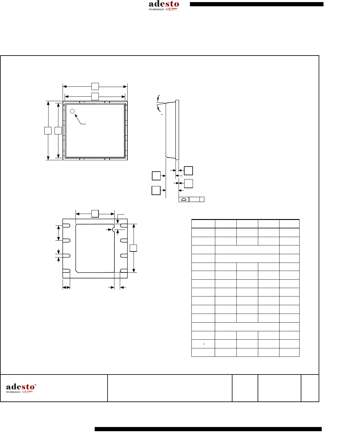
27. Packaging Information
27.1 8M1-A – MLF (VDFN)
TITLE
DRAWING NO. GPC
REV.
Package Drawing Contact:
contact@adestotech.com
8M1-A, 8-pad, 6 x 5 x 1.00mm Body, Thermally
Enhanced Plastic Very Thin Dual Flat No
Lead Package (VDFN)
D
8M1-AYBR
COMMON DIMENSIONS
(Unit of Measure = mm)
SYMBOL
MIN
NOM
MAX
NOTE
A – 0.85 1.00
A1 – – 0.05
A2 0.65 TYP
A3 0.20 TYP
b 0.35 0.40 0.48
D 5.90 6.00 6.10
D1 5.70 5.75 5.80
D2 3.20 3.40 3.60
E 4.90 5.00 5.10
E1 4.70 4.75 4.80
E2 3.80 4.00 4.20
e 1.27
L 0.50 0.60 0.75
– – 12
o
K 0.25 – –
Pin 1 ID
TOP VIEW
Pin #1 Notch
(0.20 R)
BOTTOM VIEW
D2
E2
L
b
D1
D
E1
E
e
A3
A2
A1
A
0.08
C
0
SIDE VIEW
0
K
0.45
8/28/08