
User guide
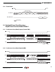
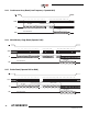
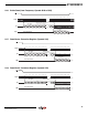
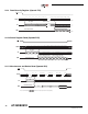
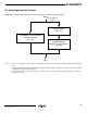
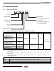
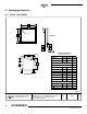
Table Of Contents
- Features
- 1. Description
- 2. Pin Configurations and Pinouts
- 3. Block Diagram
- 4. Memory Array
- 5. Device Operation
- 6. Read Commands
- 7. Program and Erase Commands
- 8. Sector Protection
- 9. Hardware Controlled Protection
- 10. Security Features
- 11. Additional Commands
- 12. Deep Power-down
- 13. “Power of 2” Binary Page Size Option
- 14. Manufacturer and Device ID Read
- 15. Command Tables
- 16. Power-on/Reset State
- 17. System Considerations
- 18. Electrical Specifications
- 19. Input Test Waveforms and Measurement Levels
- 20. Output Test Load
- 21. AC Waveforms
- 21.1 Waveform 1 – SPI Mode 0 Compatible (for Frequencies up to 66MHz)
- 21.2 Waveform 2 – SPI Mode 3 Compatible (for Frequencies up to 66MHz)
- 21.3 Waveform 3 – RapidS Mode 0 (FMAX = 66MHz)
- 21.4 Waveform 4 – RapidS Mode 3 (FMAX = 66MHz)
- 21.5 Utilizing the RapidS Function
- 21.6 Reset Timing
- 21.7 Command Sequence for Read/Write Operations for Page Size 256-Bytes (Except Status Register Read, Manufacturer and Device ID Read)
- 21.8 Command Sequence for Read/Write Operations for Page Size 264-Bytes (Except Status Register Read, Manufacturer and Device ID Read)
- 22. Write Operations
- 23. Read Operations
- 24. Detailed Bit-level Read Waveform – RapidS Serial Interface Mode 0/Mode 3
- 24.1 Continuous Array Read (Legacy Opcode E8H)
- 24.2 Continuous Array Read (Opcode 0BH)
- 24.3 Continuous Array Read (Low Frequency: Opcode 03H)
- 24.4 Main Memory Page Read (Opcode: D2H)
- 24.5 Buffer Read (Opcode D4H or D6H)
- 24.6 Buffer Read (Low Frequency: Opcode D1H or D3H)
- 24.7 Read Sector Protection Register (Opcode 32H)
- 24.8 Read Sector Lockdown Register (Opcode 35H)
- 24.9 Read Security Register (Opcode 77H)
- 24.10 Status Register Read (Opcode D7H)
- 24.11 Manufacturer and Device Read (Opcode 9FH)
- 25. Auto Page Rewrite Flowchart
- 26. Ordering Information
- 27. Packaging Information
- 28. Revision History
- 29. Errata
47
3596N–DFLASH–11/2012
AT45DB081D
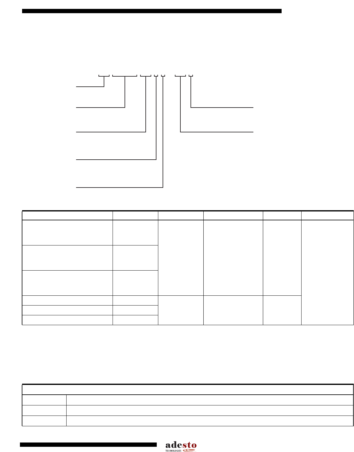
26. Ordering Information
26.1 Ordering Code Detail
Notes: 1. The shipping carrier option is not marked on the devices.
2. Standard parts are shipped with the page size set to 264-bytes. The user is able to configure these parts to a 256-byte page
size if desired.
3. Parts ordered with suffix SL954 are shipped in bulk with the page size set to 256-bytes. Parts will have a 954 or SL954
marked on them.
4. Parts ordered with suffix SL955 are shipped in tape and reel with the page size set to 256-bytes. Parts will have a 954 or
SL954 marked on them.
A T 4 5 D 0 8 S S U1D–B
Designator
Product Family
Device Density
8 = 8-megabit
Interface
1 = Serial
Package Option
M = 8-pad, 6 x 5 x 1mm MLF (VDFN)
SS = 8-lead, 0.150" wide SOIC
S = 8-lead, 0.209" wide SOIC
Device Grade
U = Matte Sn lead finish, industrial
temperature range (-40°C to +85°C)
Device Revision
26.2 Green Package Options (Pb/Halide-free/RoHS Compliant)
Ordering Code
(1)(2)
Package Lead Finish Operating Voltage f
SCK
(MHz) Operation Range
AT45DB081D-MU
AT45DB081D-MU-SL954
(3)
AT45DB081D-MU-SL955
(4)
8M1-A
Matte Sn 2.7V to 3.6V 66
Industrial
(-40Cto85C)
AT45DB081D-SSU
AT45DB081D-SSU-SL954
(3)
AT45DB081D-SSU-SL955
(4)
8S1
AT45DB081D-SU
AT45DB081D-SU-SL954
(3)
AT45DB081D-SU-SL955
(4)
8S2
AT45DB081D-MU-2.5 8M1-A
Matte Sn 2.5V to 3.6V 50AT45DB081D-SSU-2.5 8S1
AT45DB081D-SU-2.5 8S2
Package Type
8M1-A 8-pad,6x5x1.00mm Body, Very Thin Dual Flat Package No Lead MLF
™
(VDFN)
8S1 8-lead, 0.150” Wide, Plastic Gull Wing Small Outline Package (JEDEC SOIC)
8S2 8-lead, 0.209” Wide, Plastic Gull Wing Small Outline Package (EIAJ SOIC)