
User guide
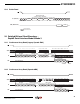
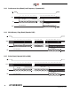
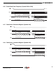
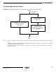
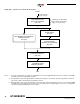
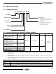
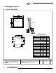
Table Of Contents
- Features
- 1. Description
- 2. Pin Configurations and Pinouts
- 3. Block Diagram
- 4. Memory Array
- 5. Device Operation
- 6. Read Commands
- 7. Program and Erase Commands
- 8. Sector Protection
- 9. Hardware Controlled Protection
- 10. Security Features
- 11. Additional Commands
- 12. Deep Power-down
- 13. “Power of 2” Binary Page Size Option
- 14. Manufacturer and Device ID Read
- 15. Command Tables
- 16. Power-on/Reset State
- 17. System Considerations
- 18. Electrical Specifications
- 19. Input Test Waveforms and Measurement Levels
- 20. Output Test Load
- 21. AC Waveforms
- 21.1 Waveform 1 – SPI Mode 0 Compatible (for Frequencies up to 66MHz)
- 21.2 Waveform 2 – SPI Mode 3 Compatible (for Frequencies up to 66MHz)
- 21.3 Waveform 3 – RapidS Mode 0 (FMAX = 66MHz)
- 21.4 Waveform 4 – RapidS Mode 3 (FMAX = 66MHz)
- 21.5 Utilizing the RapidS Function
- 21.6 Reset Timing
- 21.7 Command Sequence for Read/Write Operations for Page Size 256-Bytes (Except Status Register Read, Manufacturer and Device ID Read)
- 21.8 Command Sequence for Read/Write Operations for Page Size 264-Bytes (Except Status Register Read, Manufacturer and Device ID Read)
- 22. Write Operations
- 23. Read Operations
- 24. Detailed Bit-level Read Waveform – RapidS Serial Interface Mode 0/Mode 3
- 24.1 Continuous Array Read (Legacy Opcode E8H)
- 24.2 Continuous Array Read (Opcode 0BH)
- 24.3 Continuous Array Read (Low Frequency: Opcode 03H)
- 24.4 Main Memory Page Read (Opcode: D2H)
- 24.5 Buffer Read (Opcode D4H or D6H)
- 24.6 Buffer Read (Low Frequency: Opcode D1H or D3H)
- 24.7 Read Sector Protection Register (Opcode 32H)
- 24.8 Read Sector Lockdown Register (Opcode 35H)
- 24.9 Read Security Register (Opcode 77H)
- 24.10 Status Register Read (Opcode D7H)
- 24.11 Manufacturer and Device Read (Opcode 9FH)
- 25. Auto Page Rewrite Flowchart
- 26. Ordering Information
- 27. Packaging Information
- 28. Revision History
- 29. Errata
41
3596N–DFLASH–11/2012
AT45DB081D
23.3 Buffer Read
24. Detailed Bit-level Read Waveform –
RapidS Serial Interface Mode 0/Mode 3
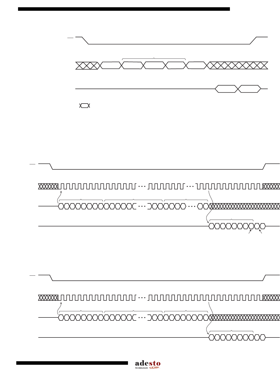
24.1 Continuous Array Read (Legacy Opcode E8H)
24.2 Continuous Array Read (Opcode 0BH)
CMD
CS
n n+1
X
X
1 Dummy Byte
X..X, BFA9-8
BFA7- 0
BINARY PAGE SIZE
15 DON'T CARE + BFA8-BFA0
Each transition
represents 8 bits
SI (INPUT)
SO (OUTPUT)
SCK
CS
SI
SO
MSB MSB
2310
11101000
675410119812 63666765646233 3431 3229 30 68 71 727069
OPCODE
AAAA AAAAA
MSB
XXXX XX
MSB MSB
DDDDDDDDDD
ADDRESS BITS 32 DON'T CARE BITS
DATA BYTE 1
HIGH-IMPEDANCE
BIT 2047/2111
OF PAGE n
BIT 0 OF
PAGE n+1
SCK
CS
SI
SO
MSB MSB
2310
00001011
675410119812 39424341403833 3431 3229 30 44 47 484645
OPCODE
AAAA AAAAA
MSB
XXXX XX
MSB MSB
DDDDDDDDDD
ADDRESS BITS A19 - A0 DON'T CARE
DATA BYTE 1
HIGH-IMPEDANCE
36 3735
X
X