
User guide
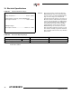
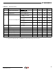
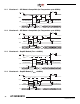
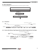
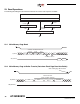
Table Of Contents
- Features
- 1. Description
- 2. Pin Configurations and Pinouts
- 3. Block Diagram
- 4. Memory Array
- 5. Device Operation
- 6. Read Commands
- 7. Program and Erase Commands
- 8. Sector Protection
- 9. Hardware Controlled Protection
- 10. Security Features
- 11. Additional Commands
- 12. Deep Power-down
- 13. “Power of 2” Binary Page Size Option
- 14. Manufacturer and Device ID Read
- 15. Command Tables
- 16. Power-on/Reset State
- 17. System Considerations
- 18. Electrical Specifications
- 19. Input Test Waveforms and Measurement Levels
- 20. Output Test Load
- 21. AC Waveforms
- 21.1 Waveform 1 – SPI Mode 0 Compatible (for Frequencies up to 66MHz)
- 21.2 Waveform 2 – SPI Mode 3 Compatible (for Frequencies up to 66MHz)
- 21.3 Waveform 3 – RapidS Mode 0 (FMAX = 66MHz)
- 21.4 Waveform 4 – RapidS Mode 3 (FMAX = 66MHz)
- 21.5 Utilizing the RapidS Function
- 21.6 Reset Timing
- 21.7 Command Sequence for Read/Write Operations for Page Size 256-Bytes (Except Status Register Read, Manufacturer and Device ID Read)
- 21.8 Command Sequence for Read/Write Operations for Page Size 264-Bytes (Except Status Register Read, Manufacturer and Device ID Read)
- 22. Write Operations
- 23. Read Operations
- 24. Detailed Bit-level Read Waveform – RapidS Serial Interface Mode 0/Mode 3
- 24.1 Continuous Array Read (Legacy Opcode E8H)
- 24.2 Continuous Array Read (Opcode 0BH)
- 24.3 Continuous Array Read (Low Frequency: Opcode 03H)
- 24.4 Main Memory Page Read (Opcode: D2H)
- 24.5 Buffer Read (Opcode D4H or D6H)
- 24.6 Buffer Read (Low Frequency: Opcode D1H or D3H)
- 24.7 Read Sector Protection Register (Opcode 32H)
- 24.8 Read Sector Lockdown Register (Opcode 35H)
- 24.9 Read Security Register (Opcode 77H)
- 24.10 Status Register Read (Opcode D7H)
- 24.11 Manufacturer and Device Read (Opcode 9FH)
- 25. Auto Page Rewrite Flowchart
- 26. Ordering Information
- 27. Packaging Information
- 28. Revision History
- 29. Errata

35
3596N–DFLASH–11/2012
AT45DB081D
19. Input Test Waveforms and Measurement Levels
t
R
,t
F
< 2 ns (10% to 90%)
20. Output Test Load
21. AC Waveforms
Six different timing waveforms are shown on page 36. Waveform 1 shows the SCK signal being
low when CS makes a high-to-low transition, and waveform 2 shows the SCK signal being high
when CS makes a high-to-low transition. In both cases, output SO becomes valid while the
SCK signal is still low (SCK low time is specified as t
WL
). Timing waveforms 1 and 2 conform to
RapidS serial interface but for frequencies up to 66MHz. Waveforms 1 and 2 are compatible with
SPI Mode 0 and SPI Mode 3, respectively.
Waveform 3 and waveform 4 illustrate general timing diagram for RapidS serial interface. These
are similar to waveform 1 and waveform 2, except that output SO is not restricted to become
valid during the t
WL
period. These timing waveforms are valid over the full frequency range (max-
imum frequency = 66MHz) of the RapidS serial case.
AC
DRIVING
LEVELS
AC
MEASUREMENT
LEVEL
0.45V
1.5V
2.4V
DEVICE
UNDER
TEST
30pF