
User guide
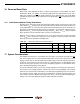
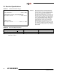
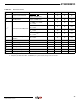
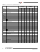
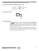
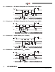
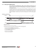
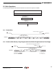
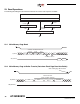
Table Of Contents
- Features
- 1. Description
- 2. Pin Configurations and Pinouts
- 3. Block Diagram
- 4. Memory Array
- 5. Device Operation
- 6. Read Commands
- 7. Program and Erase Commands
- 8. Sector Protection
- 9. Hardware Controlled Protection
- 10. Security Features
- 11. Additional Commands
- 12. Deep Power-down
- 13. “Power of 2” Binary Page Size Option
- 14. Manufacturer and Device ID Read
- 15. Command Tables
- 16. Power-on/Reset State
- 17. System Considerations
- 18. Electrical Specifications
- 19. Input Test Waveforms and Measurement Levels
- 20. Output Test Load
- 21. AC Waveforms
- 21.1 Waveform 1 – SPI Mode 0 Compatible (for Frequencies up to 66MHz)
- 21.2 Waveform 2 – SPI Mode 3 Compatible (for Frequencies up to 66MHz)
- 21.3 Waveform 3 – RapidS Mode 0 (FMAX = 66MHz)
- 21.4 Waveform 4 – RapidS Mode 3 (FMAX = 66MHz)
- 21.5 Utilizing the RapidS Function
- 21.6 Reset Timing
- 21.7 Command Sequence for Read/Write Operations for Page Size 256-Bytes (Except Status Register Read, Manufacturer and Device ID Read)
- 21.8 Command Sequence for Read/Write Operations for Page Size 264-Bytes (Except Status Register Read, Manufacturer and Device ID Read)
- 22. Write Operations
- 23. Read Operations
- 24. Detailed Bit-level Read Waveform – RapidS Serial Interface Mode 0/Mode 3
- 24.1 Continuous Array Read (Legacy Opcode E8H)
- 24.2 Continuous Array Read (Opcode 0BH)
- 24.3 Continuous Array Read (Low Frequency: Opcode 03H)
- 24.4 Main Memory Page Read (Opcode: D2H)
- 24.5 Buffer Read (Opcode D4H or D6H)
- 24.6 Buffer Read (Low Frequency: Opcode D1H or D3H)
- 24.7 Read Sector Protection Register (Opcode 32H)
- 24.8 Read Sector Lockdown Register (Opcode 35H)
- 24.9 Read Security Register (Opcode 77H)
- 24.10 Status Register Read (Opcode D7H)
- 24.11 Manufacturer and Device Read (Opcode 9FH)
- 25. Auto Page Rewrite Flowchart
- 26. Ordering Information
- 27. Packaging Information
- 28. Revision History
- 29. Errata
34
3596N–DFLASH–11/2012
AT45DB081D
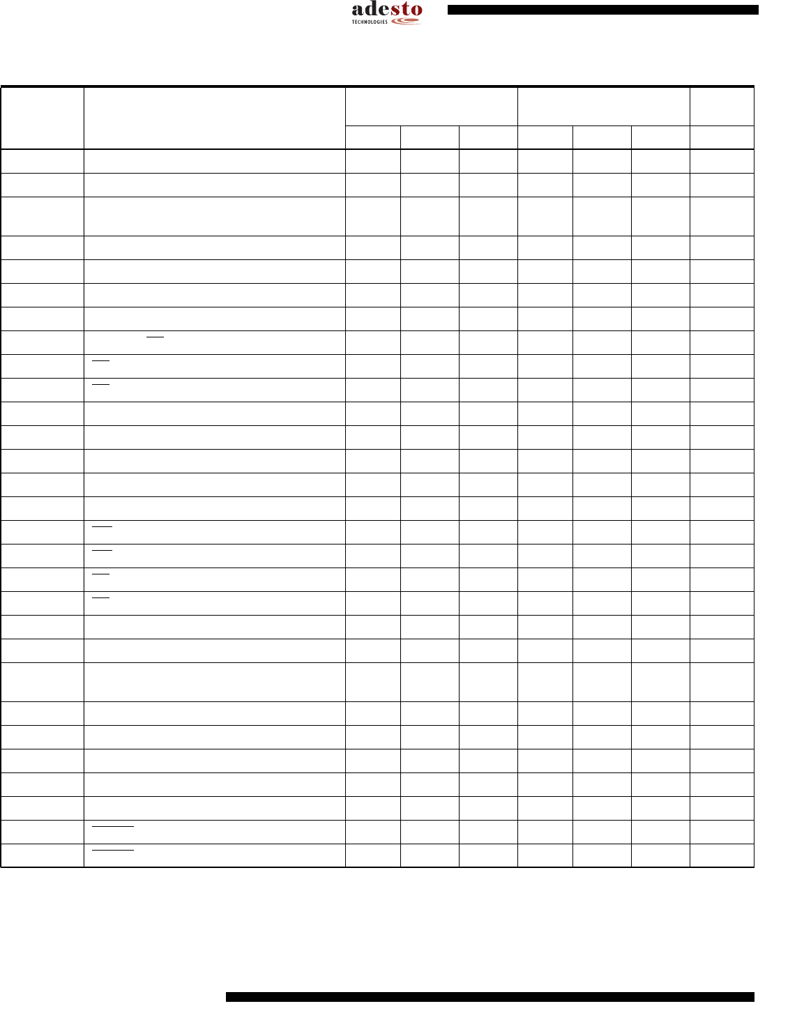
Table 18-4. AC Characteristics – RapidS/Serial Interface
Symbol Parameter
AT45DB081D
(2.5V Version) AT45DB081D
Min Typ Max Min Typ Max Units
f
SCK
SCK Frequency 50 66 MHz
f
CAR1
SCK Frequency for Continuous Array Read 50 66 MHz
f
CAR2
SCK Frequency for Continuous Array Read
(Low Frequency)
33 33 MHz
t
WH
SCK High Time 6.8 6.8 ns
t
WL
SCK Low Time 6.8 6.8 ns
t
SCKR
(1)
SCK Rise Time, Peak-to-Peak (Slew Rate) 0.1 0.1 V/ns
t
SCKF
(1)
SCK Fall Time, Peak-to-Peak (Slew Rate) 0.1 0.1 V/ns
t
CS
Minimum CS High Time 50 50 ns
t
CSS
CS Setup Time 5 5 ns
t
CSH
CS Hold Time 5 5 ns
t
SU
Data In Setup Time 2 2 ns
t
H
Data In Hold Time 3 3 ns
t
HO
Output Hold Time 0 0 ns
t
DIS
Output Disable Time 27 35 27 35 ns
t
V
Output Valid 8 6 ns
t
WPE
WP Low to Protection Enabled 1 1 µs
t
WPD
WP High to Protection Disabled 1 1 µs
t
EDPD
CS High to Deep Power-down Mode 3 3 µs
t
RDPD
CS High to Standby Mode 35 35 µs
t
XFR
Page to Buffer Transfer Time 200 200 µs
t
comp
Page to Buffer Compare Time 200 200 µs
t
EP
Page Erase and Programming Time
(256-/264-bytes)
14 35 14 35 ms
t
P
Page Programming Time (256-/264-bytes) 2 4 2 4 ms
t
PE
Page Erase Time (256-/264-bytes) 13 32 13 32 ms
t
BE
Block Erase Time (2,048-/2,112-bytes) 30 75 30 75 ms
t
SE
Sector Erase Time (65,536/67,584) 0.7 1.3 0.7 1.3 s
t
CE
Chip Erase Time 7 22 7 22 s
t
RST
RESET Pulse Width 10 10 µs
t
REC
RESET Recovery Time 1 1 µs