
User guide
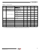
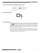
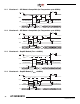
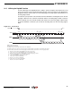
Table Of Contents
- Features
- 1. Description
- 2. Pin Configurations and Pinouts
- 3. Block Diagram
- 4. Memory Array
- 5. Device Operation
- 6. Read Commands
- 7. Program and Erase Commands
- 8. Sector Protection
- 9. Hardware Controlled Protection
- 10. Security Features
- 11. Additional Commands
- 12. Deep Power-down
- 13. “Power of 2” Binary Page Size Option
- 14. Manufacturer and Device ID Read
- 15. Command Tables
- 16. Power-on/Reset State
- 17. System Considerations
- 18. Electrical Specifications
- 19. Input Test Waveforms and Measurement Levels
- 20. Output Test Load
- 21. AC Waveforms
- 21.1 Waveform 1 – SPI Mode 0 Compatible (for Frequencies up to 66MHz)
- 21.2 Waveform 2 – SPI Mode 3 Compatible (for Frequencies up to 66MHz)
- 21.3 Waveform 3 – RapidS Mode 0 (FMAX = 66MHz)
- 21.4 Waveform 4 – RapidS Mode 3 (FMAX = 66MHz)
- 21.5 Utilizing the RapidS Function
- 21.6 Reset Timing
- 21.7 Command Sequence for Read/Write Operations for Page Size 256-Bytes (Except Status Register Read, Manufacturer and Device ID Read)
- 21.8 Command Sequence for Read/Write Operations for Page Size 264-Bytes (Except Status Register Read, Manufacturer and Device ID Read)
- 22. Write Operations
- 23. Read Operations
- 24. Detailed Bit-level Read Waveform – RapidS Serial Interface Mode 0/Mode 3
- 24.1 Continuous Array Read (Legacy Opcode E8H)
- 24.2 Continuous Array Read (Opcode 0BH)
- 24.3 Continuous Array Read (Low Frequency: Opcode 03H)
- 24.4 Main Memory Page Read (Opcode: D2H)
- 24.5 Buffer Read (Opcode D4H or D6H)
- 24.6 Buffer Read (Low Frequency: Opcode D1H or D3H)
- 24.7 Read Sector Protection Register (Opcode 32H)
- 24.8 Read Sector Lockdown Register (Opcode 35H)
- 24.9 Read Security Register (Opcode 77H)
- 24.10 Status Register Read (Opcode D7H)
- 24.11 Manufacturer and Device Read (Opcode 9FH)
- 25. Auto Page Rewrite Flowchart
- 26. Ordering Information
- 27. Packaging Information
- 28. Revision History
- 29. Errata
32
3596N–DFLASH–11/2012
AT45DB081D
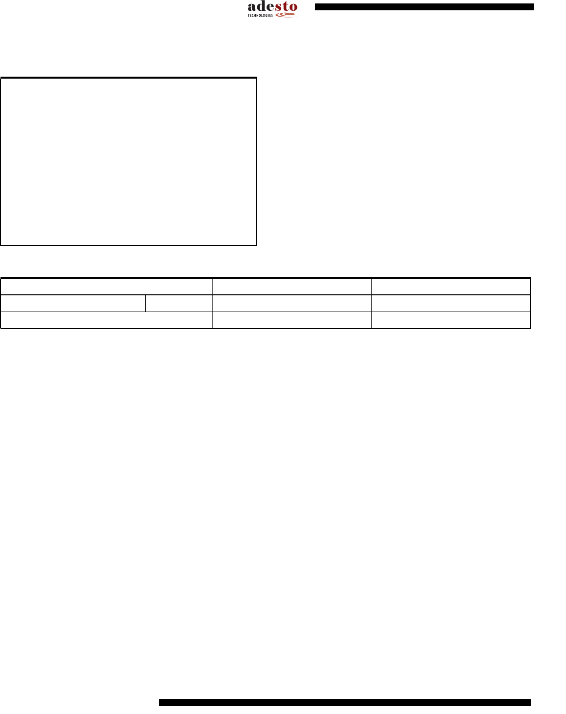
18. Electrical Specifications
Note: 1. After power is applied and V
CC
is at the minimum specified datasheet value, the system should wait 10 ms before an opera-
tional mode is started
Table 18-1. Absolute Maximum Ratings*
Temperature under Bias................................ -55C to +125C
*NOTICE: Stresses beyond those listed under “Absolute
Maximum Ratings” may cause permanent dam-
age to the device. The "Absolute Maximum Rat-
ings" are stress ratings only and functional
operation of the device at these or any other con-
ditions beyond those indicated in the operational
sections of this specification is not implied. Expo-
sure to absolute maximum rating conditions for
extended periods may affect device reliability.
Voltage Extremes referenced in the "Absolute
Maximum Ratings" are intended to accommo-
date short duration undershoot/overshoot condi-
tions and does not imply or guarantee functional
device operation at these levels for any extended
period of time
Storage Temperature..................................... -65C to +150C
All Input Voltages (except V
CC
but including NC pins)
with Respect to Ground ...................................-0.6V to +6.25V
All Output Voltages
with Respect to Ground .............................-0.6V to V
CC
+ 0.6V
Table 18-2. DC and AC Operating Range
AT45DB081D (2.5V Version) AT45DB081D
Operating Temperature (Case) Ind. -40Cto85C -40Cto85C
V
CC
Power Supply 2.5V to 3.6V 2.7V to 3.6V