
User guide
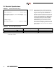
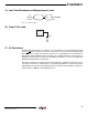
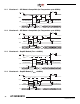
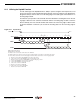
Table Of Contents
- Features
- 1. Description
- 2. Pin Configurations and Pinouts
- 3. Block Diagram
- 4. Memory Array
- 5. Device Operation
- 6. Read Commands
- 7. Program and Erase Commands
- 8. Sector Protection
- 9. Hardware Controlled Protection
- 10. Security Features
- 11. Additional Commands
- 12. Deep Power-down
- 13. “Power of 2” Binary Page Size Option
- 14. Manufacturer and Device ID Read
- 15. Command Tables
- 16. Power-on/Reset State
- 17. System Considerations
- 18. Electrical Specifications
- 19. Input Test Waveforms and Measurement Levels
- 20. Output Test Load
- 21. AC Waveforms
- 21.1 Waveform 1 – SPI Mode 0 Compatible (for Frequencies up to 66MHz)
- 21.2 Waveform 2 – SPI Mode 3 Compatible (for Frequencies up to 66MHz)
- 21.3 Waveform 3 – RapidS Mode 0 (FMAX = 66MHz)
- 21.4 Waveform 4 – RapidS Mode 3 (FMAX = 66MHz)
- 21.5 Utilizing the RapidS Function
- 21.6 Reset Timing
- 21.7 Command Sequence for Read/Write Operations for Page Size 256-Bytes (Except Status Register Read, Manufacturer and Device ID Read)
- 21.8 Command Sequence for Read/Write Operations for Page Size 264-Bytes (Except Status Register Read, Manufacturer and Device ID Read)
- 22. Write Operations
- 23. Read Operations
- 24. Detailed Bit-level Read Waveform – RapidS Serial Interface Mode 0/Mode 3
- 24.1 Continuous Array Read (Legacy Opcode E8H)
- 24.2 Continuous Array Read (Opcode 0BH)
- 24.3 Continuous Array Read (Low Frequency: Opcode 03H)
- 24.4 Main Memory Page Read (Opcode: D2H)
- 24.5 Buffer Read (Opcode D4H or D6H)
- 24.6 Buffer Read (Low Frequency: Opcode D1H or D3H)
- 24.7 Read Sector Protection Register (Opcode 32H)
- 24.8 Read Sector Lockdown Register (Opcode 35H)
- 24.9 Read Security Register (Opcode 77H)
- 24.10 Status Register Read (Opcode D7H)
- 24.11 Manufacturer and Device Read (Opcode 9FH)
- 25. Auto Page Rewrite Flowchart
- 26. Ordering Information
- 27. Packaging Information
- 28. Revision History
- 29. Errata
31
3596N–DFLASH–11/2012
AT45DB081D
16. Power-on/Reset State
When power is first applied to the device, or when recovering from a reset condition, the device
will default to Mode 3. In addition, the output pin (SO) will be in a high impedance state, and a
high-to-low transition on the
CS pin will be required to start a valid instruction. The mode (Mode
3 or Mode 0) will be automatically selected on every falling edge of
CS by sampling the inactive
clock state.
16.1 Initial Power-up/Reset Timing Restrictions
At power up, the device must not be selected until the supply voltage reaches the V
CC
(min.) and
further delay of t
VCSL
. During power-up, the internal Power-on Reset circuitry keeps the device in
reset mode until the V
CC
rises above the Power-on Reset threshold value (V
POR
). At this time, all
operations are disabled and the device does not respond to any commands. After power up is
applied and the V
CC
is at the minimum operating voltage V
CC
(min.), the t
VCSL
delay is required
before the device can be selected in order to perform a read operation.
Similarly, the t
PUW
delay is required after the V
CC
rises above the Power-on Reset threshold
value (V
POR
) before the device can perform a write (Program or Erase) operation. After initial
power-up, the device will default in Standby mode.
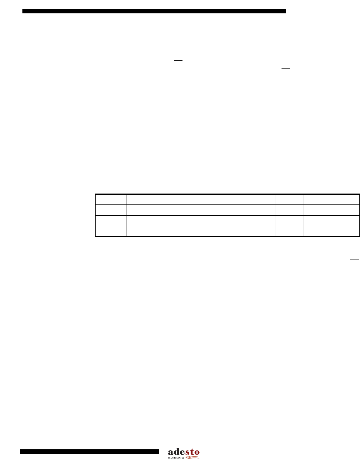
Table 16-1. Initial Power-up/Reset Timing Restrictions
17. System Considerations
The RapidS serial interface is controlled by the clock SCK, serial input SI and chip select CS
pins. These signals must rise and fall monotonically and be free from noise. Excessive noise or
ringing on these pins can be misinterpreted as multiple edges and cause improper operation of
the device. The PC board traces must be kept to a minimum distance or appropriately termi-
nated to ensure proper operation. If necessary, decoupling capacitors can be added on these
pins to provide filtering against noise glitches.
As system complexity continues to increase, voltage regulation is becoming more important. A
key element of any voltage regulation scheme is its current sourcing capability. Like all Flash
memories, the peak current for DataFlash occur during the programming and erase operation.
The regulator needs to supply this peak current requirement. An under specified regulator can
cause current starvation. Besides increasing system noise, current starvation during program-
ming or erase can lead to improper operation and possible data corruption.
Symbol Parameter Min Typ Max Units
t
VCSL
V
CC
(min.) to Chip Select low 70 µs
t
PUW
Power-Up Device Delay before Write Allowed 20 ms
V
POR
Power-ON Reset Voltage 1.5 2.5 V