
User guide
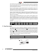
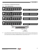
Table Of Contents
- Features
- 1. Description
- 2. Pin Configurations and Pinouts
- 3. Block Diagram
- 4. Memory Array
- 5. Device Operation
- 6. Read Commands
- 7. Program and Erase Commands
- 8. Sector Protection
- 9. Hardware Controlled Protection
- 10. Security Features
- 11. Additional Commands
- 12. Deep Power-down
- 13. “Power of 2” Binary Page Size Option
- 14. Manufacturer and Device ID Read
- 15. Command Tables
- 16. Power-on/Reset State
- 17. System Considerations
- 18. Electrical Specifications
- 19. Input Test Waveforms and Measurement Levels
- 20. Output Test Load
- 21. AC Waveforms
- 21.1 Waveform 1 – SPI Mode 0 Compatible (for Frequencies up to 66MHz)
- 21.2 Waveform 2 – SPI Mode 3 Compatible (for Frequencies up to 66MHz)
- 21.3 Waveform 3 – RapidS Mode 0 (FMAX = 66MHz)
- 21.4 Waveform 4 – RapidS Mode 3 (FMAX = 66MHz)
- 21.5 Utilizing the RapidS Function
- 21.6 Reset Timing
- 21.7 Command Sequence for Read/Write Operations for Page Size 256-Bytes (Except Status Register Read, Manufacturer and Device ID Read)
- 21.8 Command Sequence for Read/Write Operations for Page Size 264-Bytes (Except Status Register Read, Manufacturer and Device ID Read)
- 22. Write Operations
- 23. Read Operations
- 24. Detailed Bit-level Read Waveform – RapidS Serial Interface Mode 0/Mode 3
- 24.1 Continuous Array Read (Legacy Opcode E8H)
- 24.2 Continuous Array Read (Opcode 0BH)
- 24.3 Continuous Array Read (Low Frequency: Opcode 03H)
- 24.4 Main Memory Page Read (Opcode: D2H)
- 24.5 Buffer Read (Opcode D4H or D6H)
- 24.6 Buffer Read (Low Frequency: Opcode D1H or D3H)
- 24.7 Read Sector Protection Register (Opcode 32H)
- 24.8 Read Sector Lockdown Register (Opcode 35H)
- 24.9 Read Security Register (Opcode 77H)
- 24.10 Status Register Read (Opcode D7H)
- 24.11 Manufacturer and Device Read (Opcode 9FH)
- 25. Auto Page Rewrite Flowchart
- 26. Ordering Information
- 27. Packaging Information
- 28. Revision History
- 29. Errata

30
3596N–DFLASH–11/2012
AT45DB081D
Notes: P = Page Address Bit B = Byte/Buffer Address Bit x = Don’t Care
Table 15-7. Detailed Bit-level Addressing Sequence for the DataFlash Standard Page Size (264-Bytes)
Page Size = 264-bytes Address Byte Address Byte Address Byte
Additional
Don’t Care
BytesOpcode Opcode
Reserved
Reserved
Reserved
PA11
PA10
PA9
PA8
PA7
PA6
PA5
PA4
PA3
PA2
PA1
PA0
BA8
BA7
BA6
BA5
BA4
BA3
BA2
BA1
BA0
03h 0 0 0 0 0 0 1 1 x x xPPPPP PPPPPPPB BBBBBBB B
N/A
0Bh 0 0 0 0 1 0 1 1 x x xPPPP P PPPPPPP BBBBBBBB B
1
50h 01010000 xxxPPPPPPPPPxxxx xxxxxxx x
N/A
53h 0 1 0 1 0 0 1 1 x x xPPPPP PPPPPPP x x x x x x x x x
N/A
55h 0 1 0 1 0 1 0 1 x x xPPPPP PPPPPPP x x x x x x x x x
N/A
58h 0 1 0 1 1 0 0 0 x x xPPPPP PPPPPPP x x x x x x x x x
N/A
59h 0 1 0 1 1 0 0 1 x x xPPPPP PPPPPPP x x x x x x x x x
N/A
60h 0 1 1 0 0 0 0 0 x x xPPPPP PPPPPPP x x x x x x x x x
N/A
61h 0 1 1 0 0 0 0 1 x x xPPPPP PPPPPPP x x x x x x x x x
N/A
77h 01110111 xxxxxxx x xxxxxxx x xxxxxxx x
N/A
7Ch 01111100 xxxPPPx x xxxxxxx x xxxxxxx x
N/A
81h 1 0 0 0 0 0 0 1 x x xPPPPP PPPPPPP x x x x x x x x x
N/A
82h 1 0 0 0 0 0 1 0 x x xPPPPP PPPPPPPB BBBBBBB B
N/A
83h 1 0 0 0 0 0 1 1 x x xPPPPP PPPPPPP x x x x x x x x x
N/A
84h 10000100 xxxxxxx x xxxxxxxBBBBBBBBB
N/A
85h 1 0 0 0 0 1 0 1 x x xPPPPP PPPPPPPB BBBBBBB B
N/A
86h 1 0 0 0 0 1 1 0 x x xPPPPP PPPPPPP x x x x x x x x x
N/A
87h 10000111 xxxxxxx x xxxxxxxBBBBBBBBB
N/A
88h 1 0 0 0 1 0 0 0 x x xPPPPP PPPPPPP x x x x x x x x x
N/A
89h 1 0 0 0 1 0 0 1 x x xPPPPP PPPPPPP x x x x x x x x x
N/A
9Fh 1 0 0 1 1 1 1 1 N/A N/A N/A
N/A
B9h 1 0 1 1 1 0 0 1 N/A N/A N/A
N/A
ABh 1 0 1 0 1 0 1 1 N/A N/A N/A
N/A
D1h 11010001 xxxxxxx x xxxxxxxBBBBBBBB B
N/A
D2h 11 0 1 0 0 1 0 x x xPPPP P PPPPPPP B BBBBBBB B
4
D3h 11010001 xxxxxxx x xxxxxxxBBBBBBBB B
N/A
D4h 11010100 xxxxxxx x xxxxxxxBBBBBBBB B
1
D6h 11010110 xxxxxxx x xxxxxxxBBBBBBBB B
1
D7h 1 1 0 1 0 1 1 1 N/A N/A N/A
N/A
E8h 1 1 1 0 1 0 0 0 x x xPPPP P PPPPPPP BBBBBBBB B
4