
User guide
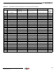
Table Of Contents
- Features
- 1. Description
- 2. Pin Configurations and Pinouts
- 3. Block Diagram
- 4. Memory Array
- 5. Device Operation
- 6. Read Commands
- 7. Program and Erase Commands
- 8. Sector Protection
- 9. Hardware Controlled Protection
- 10. Security Features
- 11. Additional Commands
- 12. Deep Power-down
- 13. “Power of 2” Binary Page Size Option
- 14. Manufacturer and Device ID Read
- 15. Command Tables
- 16. Power-on/Reset State
- 17. System Considerations
- 18. Electrical Specifications
- 19. Input Test Waveforms and Measurement Levels
- 20. Output Test Load
- 21. AC Waveforms
- 21.1 Waveform 1 – SPI Mode 0 Compatible (for Frequencies up to 66MHz)
- 21.2 Waveform 2 – SPI Mode 3 Compatible (for Frequencies up to 66MHz)
- 21.3 Waveform 3 – RapidS Mode 0 (FMAX = 66MHz)
- 21.4 Waveform 4 – RapidS Mode 3 (FMAX = 66MHz)
- 21.5 Utilizing the RapidS Function
- 21.6 Reset Timing
- 21.7 Command Sequence for Read/Write Operations for Page Size 256-Bytes (Except Status Register Read, Manufacturer and Device ID Read)
- 21.8 Command Sequence for Read/Write Operations for Page Size 264-Bytes (Except Status Register Read, Manufacturer and Device ID Read)
- 22. Write Operations
- 23. Read Operations
- 24. Detailed Bit-level Read Waveform – RapidS Serial Interface Mode 0/Mode 3
- 24.1 Continuous Array Read (Legacy Opcode E8H)
- 24.2 Continuous Array Read (Opcode 0BH)
- 24.3 Continuous Array Read (Low Frequency: Opcode 03H)
- 24.4 Main Memory Page Read (Opcode: D2H)
- 24.5 Buffer Read (Opcode D4H or D6H)
- 24.6 Buffer Read (Low Frequency: Opcode D1H or D3H)
- 24.7 Read Sector Protection Register (Opcode 32H)
- 24.8 Read Sector Lockdown Register (Opcode 35H)
- 24.9 Read Security Register (Opcode 77H)
- 24.10 Status Register Read (Opcode D7H)
- 24.11 Manufacturer and Device Read (Opcode 9FH)
- 25. Auto Page Rewrite Flowchart
- 26. Ordering Information
- 27. Packaging Information
- 28. Revision History
- 29. Errata

26
3596N–DFLASH–11/2012
AT45DB081D
14.2 Operation Mode Summary
The commands described previously can be grouped into four different categories to better
describe which commands can be executed at what times.
Group A commands consist of:
1. Main Memory Page Read
2. Continuous Array Read
3. Read Sector Protection Register
4. Read Sector Lockdown Register
5. Read Security Register
Group B commands consist of:
1. Page Erase
2. Block Erase
3. Sector Erase
4. Chip Erase
5. Main Memory Page to Buffer 1 (or 2) Transfer
6. Main Memory Page to Buffer 1 (or 2) Compare
7. Buffer 1 (or 2) to Main Memory Page Program with Built-in Erase
8. Buffer 1 (or 2) to Main Memory Page Program without Built-in Erase
9. Main Memory Page Program through Buffer 1 (or 2)
10. Auto Page Rewrite
Group C commands consist of:
1. Buffer 1 (or 2) Read
2. Buffer 1 (or 2) Write
3. Status Register Read
4. Manufacturer and Device ID Read
Group D commands consist of:
1. Erase Sector Protection Register
2. Program Sector Protection Register
3. Sector Lockdown
4. Program Security Register
If a Group A command is in progress (not fully completed), then another command in Group A,
B, C, or D should not be started. However, during the internally self-timed portion of Group B
commands, any command in Group C can be executed. The Group B commands using buffer 1
should use Group C commands using buffer 2 and vice versa. Finally, during the internally self-
timed portion of a Group D command, only the Status Register Read command should be
executed.