
User guide
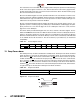
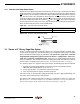
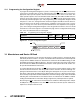
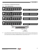
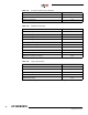
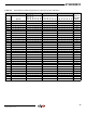
Table Of Contents
- Features
- 1. Description
- 2. Pin Configurations and Pinouts
- 3. Block Diagram
- 4. Memory Array
- 5. Device Operation
- 6. Read Commands
- 7. Program and Erase Commands
- 8. Sector Protection
- 9. Hardware Controlled Protection
- 10. Security Features
- 11. Additional Commands
- 12. Deep Power-down
- 13. “Power of 2” Binary Page Size Option
- 14. Manufacturer and Device ID Read
- 15. Command Tables
- 16. Power-on/Reset State
- 17. System Considerations
- 18. Electrical Specifications
- 19. Input Test Waveforms and Measurement Levels
- 20. Output Test Load
- 21. AC Waveforms
- 21.1 Waveform 1 – SPI Mode 0 Compatible (for Frequencies up to 66MHz)
- 21.2 Waveform 2 – SPI Mode 3 Compatible (for Frequencies up to 66MHz)
- 21.3 Waveform 3 – RapidS Mode 0 (FMAX = 66MHz)
- 21.4 Waveform 4 – RapidS Mode 3 (FMAX = 66MHz)
- 21.5 Utilizing the RapidS Function
- 21.6 Reset Timing
- 21.7 Command Sequence for Read/Write Operations for Page Size 256-Bytes (Except Status Register Read, Manufacturer and Device ID Read)
- 21.8 Command Sequence for Read/Write Operations for Page Size 264-Bytes (Except Status Register Read, Manufacturer and Device ID Read)
- 22. Write Operations
- 23. Read Operations
- 24. Detailed Bit-level Read Waveform – RapidS Serial Interface Mode 0/Mode 3
- 24.1 Continuous Array Read (Legacy Opcode E8H)
- 24.2 Continuous Array Read (Opcode 0BH)
- 24.3 Continuous Array Read (Low Frequency: Opcode 03H)
- 24.4 Main Memory Page Read (Opcode: D2H)
- 24.5 Buffer Read (Opcode D4H or D6H)
- 24.6 Buffer Read (Low Frequency: Opcode D1H or D3H)
- 24.7 Read Sector Protection Register (Opcode 32H)
- 24.8 Read Sector Lockdown Register (Opcode 35H)
- 24.9 Read Security Register (Opcode 77H)
- 24.10 Status Register Read (Opcode D7H)
- 24.11 Manufacturer and Device Read (Opcode 9FH)
- 25. Auto Page Rewrite Flowchart
- 26. Ordering Information
- 27. Packaging Information
- 28. Revision History
- 29. Errata
25
3596N–DFLASH–11/2012
AT45DB081D
14.1 Manufacturer and Device ID Information
Note: Based on JEDEC publication 106 (JEP106), Manufacturer ID data can be comprised of any number of bytes. Some manufacturers may have
Manufacturer ID codes that are two, three or even four bytes long with the first byte(s) in the sequence being 7FH. A system should detect code
7FH as a “Continuation Code” and continue to read Manufacturer ID bytes. The first non-7FH byte would signify the last byte of Manufacturer ID
data. For Adesto (and some other manufacturers), the Manufacturer ID data is comprised of only one byte.
14.1.1 Byte 1 – Manufacturer ID
Hex
Value
JEDEC Assigned Code
Bit 7 Bit 6 Bit 5 Bit 4 Bit 3 Bit 2 Bit 1 Bit 0
1FH 0 0 0 1 1 1 1 1 Manufacturer ID 1FH = Adesto
14.1.2 Byte2–DeviceID(Part1)
Hex
Value
Family Code Density Code
Bit 7 Bit 6 Bit 5 Bit 4 Bit 3 Bit 2 Bit 1 Bit 0 Family Code 001 = DataFlash
25H 0 0 1 0 0 1 0 1 Density Code 00101 = 8-Mbit
14.1.3 Byte3–DeviceID(Part2)
Hex
Value
MLC Code Product Version Code
Bit 7 Bit 6 Bit 5 Bit 4 Bit 3 Bit 2 Bit 1 Bit 0 MLC Code 000 = 1-bit/Cell Technology
00H 0 0 0 0 0 0 0 0 Product Version 00000 = Initial Version
14.1.4 Byte 4 – Extended Device Information String Length
Hex
Value
Byte Count
Bit 7 Bit 6 Bit 5 Bit 4 Bit 3 Bit 2 Bit 1 Bit 0
00H 0 0 0 0 0 0 0 0 Byte Count 00H=0Bytes of Information
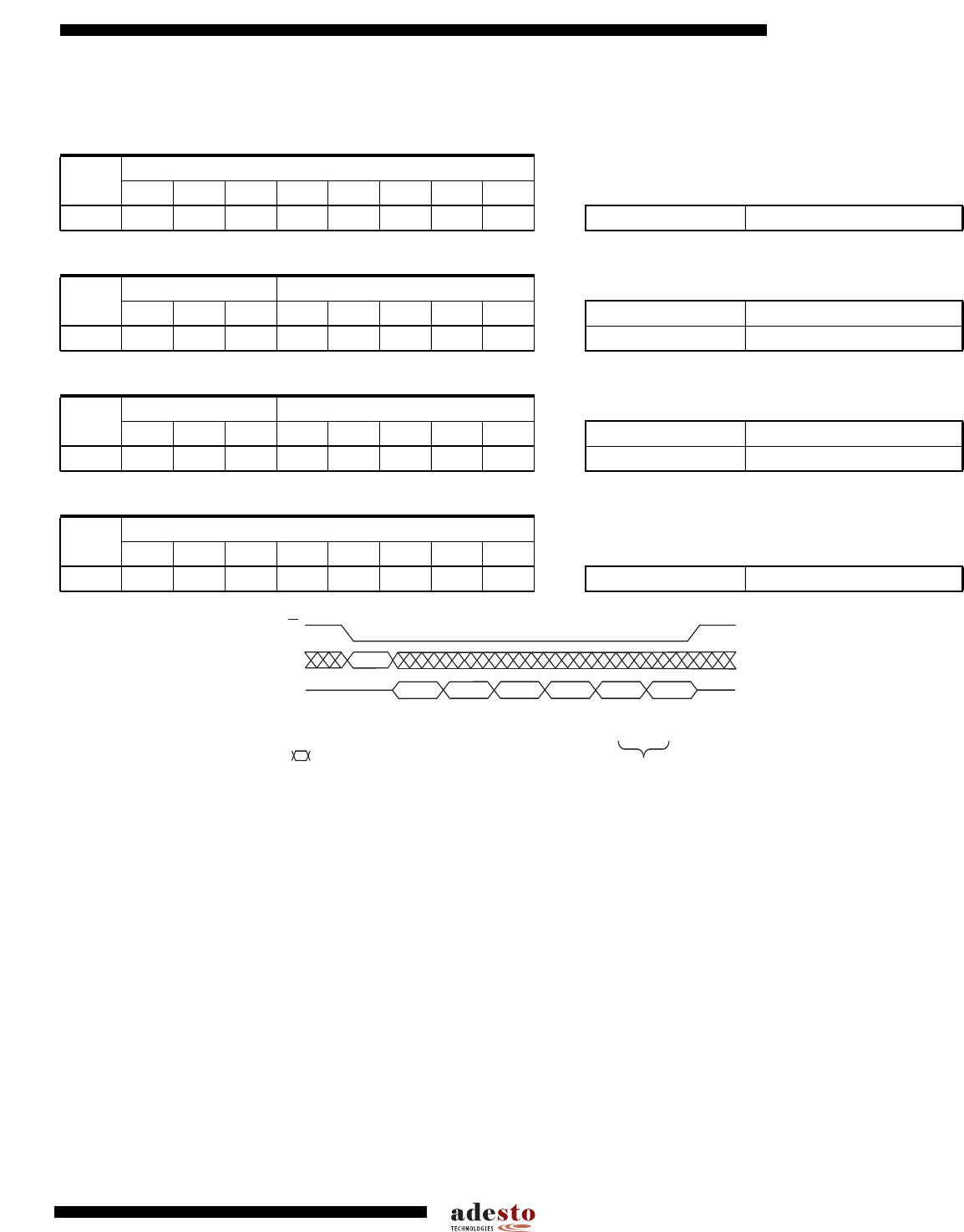
9FH
Manufacturer ID
Byte n
Device ID
Byte 1
Device ID
Byte 2
This information would only be output
if the Extended Device Information String Length
value was something other than 00H.
Extended
Device
Information
String Length
Extended
Device
Information
Byte x
Extended
Device
Information
Byte x + 1
CS
1FH
25H 00H
00H Data Data
SI
SO
Opcode
Each transition
represents 8 bits