
User guide
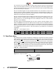
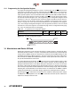
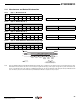
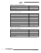
Table Of Contents
- Features
- 1. Description
- 2. Pin Configurations and Pinouts
- 3. Block Diagram
- 4. Memory Array
- 5. Device Operation
- 6. Read Commands
- 7. Program and Erase Commands
- 8. Sector Protection
- 9. Hardware Controlled Protection
- 10. Security Features
- 11. Additional Commands
- 12. Deep Power-down
- 13. “Power of 2” Binary Page Size Option
- 14. Manufacturer and Device ID Read
- 15. Command Tables
- 16. Power-on/Reset State
- 17. System Considerations
- 18. Electrical Specifications
- 19. Input Test Waveforms and Measurement Levels
- 20. Output Test Load
- 21. AC Waveforms
- 21.1 Waveform 1 – SPI Mode 0 Compatible (for Frequencies up to 66MHz)
- 21.2 Waveform 2 – SPI Mode 3 Compatible (for Frequencies up to 66MHz)
- 21.3 Waveform 3 – RapidS Mode 0 (FMAX = 66MHz)
- 21.4 Waveform 4 – RapidS Mode 3 (FMAX = 66MHz)
- 21.5 Utilizing the RapidS Function
- 21.6 Reset Timing
- 21.7 Command Sequence for Read/Write Operations for Page Size 256-Bytes (Except Status Register Read, Manufacturer and Device ID Read)
- 21.8 Command Sequence for Read/Write Operations for Page Size 264-Bytes (Except Status Register Read, Manufacturer and Device ID Read)
- 22. Write Operations
- 23. Read Operations
- 24. Detailed Bit-level Read Waveform – RapidS Serial Interface Mode 0/Mode 3
- 24.1 Continuous Array Read (Legacy Opcode E8H)
- 24.2 Continuous Array Read (Opcode 0BH)
- 24.3 Continuous Array Read (Low Frequency: Opcode 03H)
- 24.4 Main Memory Page Read (Opcode: D2H)
- 24.5 Buffer Read (Opcode D4H or D6H)
- 24.6 Buffer Read (Low Frequency: Opcode D1H or D3H)
- 24.7 Read Sector Protection Register (Opcode 32H)
- 24.8 Read Sector Lockdown Register (Opcode 35H)
- 24.9 Read Security Register (Opcode 77H)
- 24.10 Status Register Read (Opcode D7H)
- 24.11 Manufacturer and Device Read (Opcode 9FH)
- 25. Auto Page Rewrite Flowchart
- 26. Ordering Information
- 27. Packaging Information
- 28. Revision History
- 29. Errata
22
3596N–DFLASH–11/2012
AT45DB081D
The result of the most recent Main Memory Page to Buffer Compare operation is indicated using
bit six of the status register. If bit six is a zero, then the data in the main memory page matches
the data in the buffer. If bit six is a one, then at least one bit of the data in the main memory page
does not match the data in the buffer.
Bit one in the Status Register is used to provide information to the user whether or not the sector
protection has been enabled or disabled, either by software-controlled method or hardware-con-
trolled method. A logic one indicates that sector protection has been enabled and logic zero
indicates that sector protection has been disabled.
Bit zero in the Status Register indicates whether the page size of the main memory array is con-
figured for “power of 2” binary page size (256-bytes) or the DataFlash standard page size (264-
bytes). If bit zero is a one, then the page size is set to 256-bytes. If bit zero is a zero, then the
page size is set to 264-bytes.
The device density is indicated using bits five, four, three, and two of the status register. For the
Adesto AT45DB081D, the four bits are 1001 The decimal value of these four binary bits does not
equate to the device density; the four bits represent a combinational code relating to differing
densities of DataFlash devices. The device density is not the same as the density code indicated
in the JEDEC device ID information. The device density is provided only for backward
compatibility.
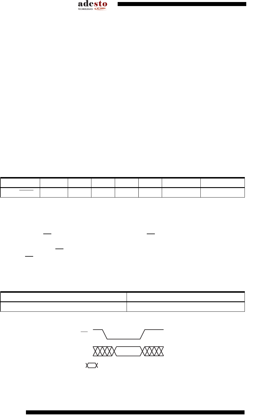
12. Deep Power-down
After initial power-up, the device will default in standby mode. The Deep Power-down command
allows the device to enter into the lowest power consumption mode. To enter the Deep Power-
down mode, the CS pin must first be asserted. Once the CS pin has been asserted, an opcode
of B9H command must be clocked in via input pin (SI). After the last bit of the command has
been clocked in, the CS pin must be de-asserted to initiate the Deep Power-down operation.
After the CS pin is de-asserted, the will device enter the Deep Power-down mode within the
maximum t
EDPD
time. Once the device has entered the Deep Power-down mode, all instructions
are ignored except for the Resume from Deep Power-down command.
Table 12-1. Deep Power-down
Figure 12-1. Deep Power-down
Table 11-1. Status Register Format
Bit 7 Bit 6 Bit 5 Bit 4 Bit 3 Bit 2 Bit 1 Bit 0
RDY/
BUSY COMP 1 0 0 1 PROTECT PAGE SIZE
Command Opcode
Deep Power-down B9H
Opcode
CS
Each transition
represents 8 bits
SI