
User guide

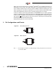


Table Of Contents
- Features
- 1. Description
- 2. Pin Configurations and Pinouts
- 3. Block Diagram
- 4. Memory Array
- 5. Device Operation
- 6. Read Commands
- 7. Program and Erase Commands
- 8. Sector Protection
- 9. Hardware Controlled Protection
- 10. Security Features
- 11. Additional Commands
- 12. Deep Power-down
- 13. “Power of 2” Binary Page Size Option
- 14. Manufacturer and Device ID Read
- 15. Command Tables
- 16. Power-on/Reset State
- 17. System Considerations
- 18. Electrical Specifications
- 19. Input Test Waveforms and Measurement Levels
- 20. Output Test Load
- 21. AC Waveforms
- 21.1 Waveform 1 – SPI Mode 0 Compatible (for Frequencies up to 66MHz)
- 21.2 Waveform 2 – SPI Mode 3 Compatible (for Frequencies up to 66MHz)
- 21.3 Waveform 3 – RapidS Mode 0 (FMAX = 66MHz)
- 21.4 Waveform 4 – RapidS Mode 3 (FMAX = 66MHz)
- 21.5 Utilizing the RapidS Function
- 21.6 Reset Timing
- 21.7 Command Sequence for Read/Write Operations for Page Size 256-Bytes (Except Status Register Read, Manufacturer and Device ID Read)
- 21.8 Command Sequence for Read/Write Operations for Page Size 264-Bytes (Except Status Register Read, Manufacturer and Device ID Read)
- 22. Write Operations
- 23. Read Operations
- 24. Detailed Bit-level Read Waveform – RapidS Serial Interface Mode 0/Mode 3
- 24.1 Continuous Array Read (Legacy Opcode E8H)
- 24.2 Continuous Array Read (Opcode 0BH)
- 24.3 Continuous Array Read (Low Frequency: Opcode 03H)
- 24.4 Main Memory Page Read (Opcode: D2H)
- 24.5 Buffer Read (Opcode D4H or D6H)
- 24.6 Buffer Read (Low Frequency: Opcode D1H or D3H)
- 24.7 Read Sector Protection Register (Opcode 32H)
- 24.8 Read Sector Lockdown Register (Opcode 35H)
- 24.9 Read Security Register (Opcode 77H)
- 24.10 Status Register Read (Opcode D7H)
- 24.11 Manufacturer and Device Read (Opcode 9FH)
- 25. Auto Page Rewrite Flowchart
- 26. Ordering Information
- 27. Packaging Information
- 28. Revision History
- 29. Errata
2
3596N–DFLASH–11/2012
AT45DB081D
address lines and a parallel interface, the Adesto
™
DataFlash
®
uses a RapidS serial interface to
sequentially access its data. The simple sequential access dramatically reduces active pin
count, facilitates hardware layout, increases system reliability, minimizes switching noise, and
reduces package size. The device is optimized for use in many commercial and industrial appli-
cations where high-density, low-pin count, low-voltage and low-power are essential.
To allow for simple in-system reprogrammability, the AT45DB081D does not require high input
voltages for programming. The device operates from a single power supply, 2.5V to 3.6V or 2.7V
to 3.6V, for both the program and read operations. The AT45DB081D is enabled through the
chip select pin (CS) and accessed via a three-wire interface consisting of the Serial Input (SI),
Serial Output (SO), and the Serial Clock (SCK).
All programming and erase cycles are self-timed.
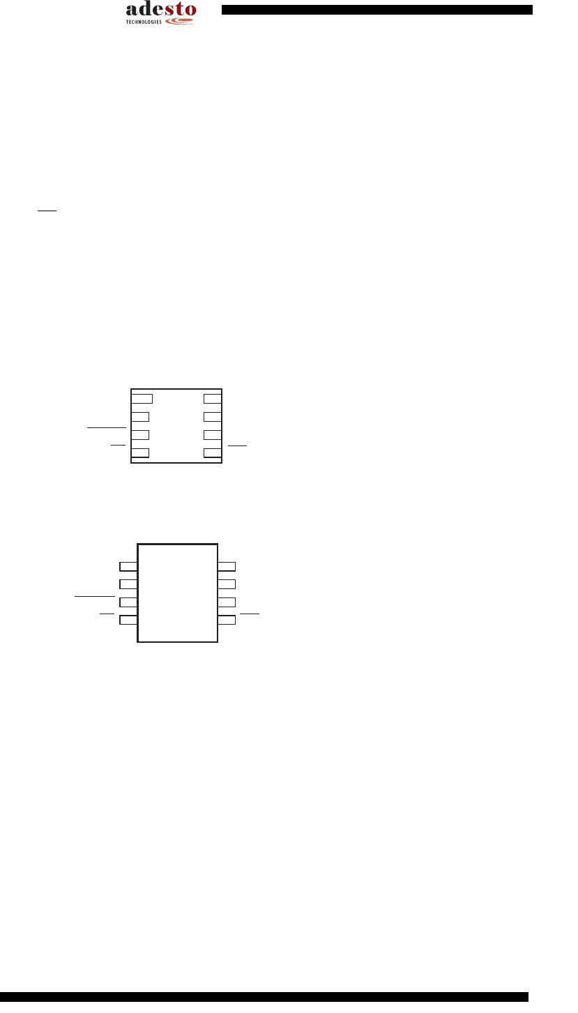
2. Pin Configurations and Pinouts
Note: 1. The metal pad on the bottom of the MLF package is floating. This pad can be a “No Connect”
or connected to GND
Figure 2-1. MLF (VDFN) Top View
Figure 2-2. SOIC Top View
SI
SCK
RESET
CS
SO
GND
VCC
WP
8
7
6
5
1
2
3
4
1
2
3
4
8
7
6
5
SI
SCK
RESET
CS
SO
GND
VCC
WP