
User guide
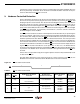
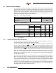
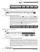
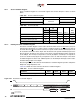
Table Of Contents
- Features
- 1. Description
- 2. Pin Configurations and Pinouts
- 3. Block Diagram
- 4. Memory Array
- 5. Device Operation
- 6. Read Commands
- 7. Program and Erase Commands
- 8. Sector Protection
- 9. Hardware Controlled Protection
- 10. Security Features
- 11. Additional Commands
- 12. Deep Power-down
- 13. “Power of 2” Binary Page Size Option
- 14. Manufacturer and Device ID Read
- 15. Command Tables
- 16. Power-on/Reset State
- 17. System Considerations
- 18. Electrical Specifications
- 19. Input Test Waveforms and Measurement Levels
- 20. Output Test Load
- 21. AC Waveforms
- 21.1 Waveform 1 – SPI Mode 0 Compatible (for Frequencies up to 66MHz)
- 21.2 Waveform 2 – SPI Mode 3 Compatible (for Frequencies up to 66MHz)
- 21.3 Waveform 3 – RapidS Mode 0 (FMAX = 66MHz)
- 21.4 Waveform 4 – RapidS Mode 3 (FMAX = 66MHz)
- 21.5 Utilizing the RapidS Function
- 21.6 Reset Timing
- 21.7 Command Sequence for Read/Write Operations for Page Size 256-Bytes (Except Status Register Read, Manufacturer and Device ID Read)
- 21.8 Command Sequence for Read/Write Operations for Page Size 264-Bytes (Except Status Register Read, Manufacturer and Device ID Read)
- 22. Write Operations
- 23. Read Operations
- 24. Detailed Bit-level Read Waveform – RapidS Serial Interface Mode 0/Mode 3
- 24.1 Continuous Array Read (Legacy Opcode E8H)
- 24.2 Continuous Array Read (Opcode 0BH)
- 24.3 Continuous Array Read (Low Frequency: Opcode 03H)
- 24.4 Main Memory Page Read (Opcode: D2H)
- 24.5 Buffer Read (Opcode D4H or D6H)
- 24.6 Buffer Read (Low Frequency: Opcode D1H or D3H)
- 24.7 Read Sector Protection Register (Opcode 32H)
- 24.8 Read Sector Lockdown Register (Opcode 35H)
- 24.9 Read Security Register (Opcode 77H)
- 24.10 Status Register Read (Opcode D7H)
- 24.11 Manufacturer and Device Read (Opcode 9FH)
- 25. Auto Page Rewrite Flowchart
- 26. Ordering Information
- 27. Packaging Information
- 28. Revision History
- 29. Errata
18
3596N–DFLASH–11/2012
AT45DB081D
10.1.1 Sector Lockdown Register
Sector Lockdown Register is a nonvolatile register that contains 16-bytes of data, as shown
below:
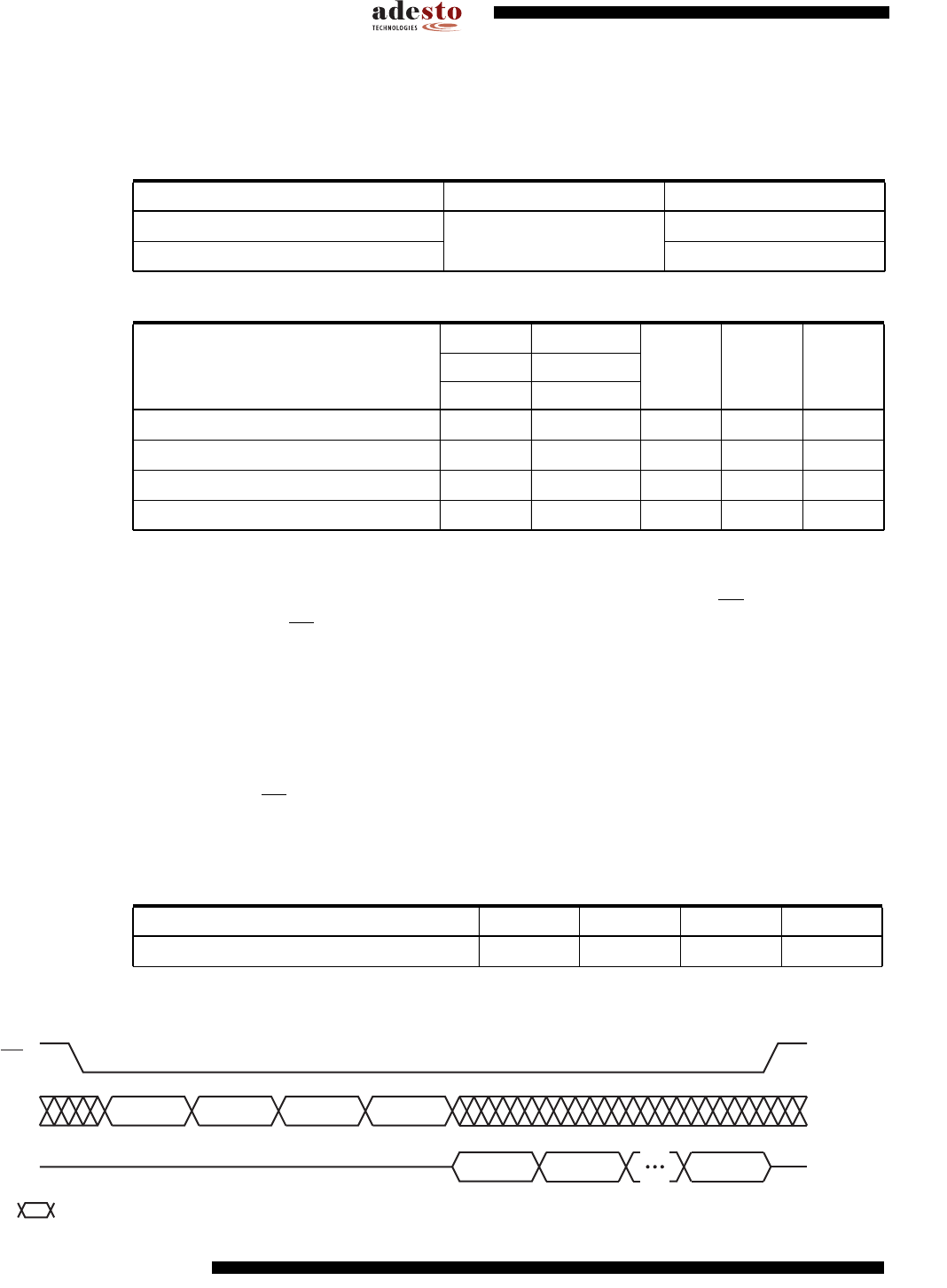
Table 10-2. Sector Lockdown Register
10.1.2 Reading the Sector Lockdown Register
The Sector Lockdown Register can be read to determine which sectors in the memory array are
permanently locked down. To read the Sector Lockdown Register, the CS pin must first be
asserted. Once the CS pin has been asserted, an opcode of 35H and three dummy bytes must
be clocked into the device via the SI pin. After the last bit of the opcode and dummy bytes have
been clocked in, the data for the contents of the Sector Lockdown Register will be clocked out
on the SO pin. The first byte corresponds to sector 0 (0a, 0b) the second byte corresponds to
sector one and the las byte (byte 16) corresponds to sector 15. After the last byte of the Sector
Lockdown Register has been read, additional pulses on the SCK pin will simply result in unde-
fined data being output on the SO pin.
Deasserting the CS pin will terminate the Read Sector Lockdown Register operation and put the
SO pin into a high-impedance state.
Table 10-4 details the values read from the Sector Lockdown Register.
Figure 10-2. Read Sector Lockdown Register
Sector Number 0 (0a, 0b) 1 to 15
Locked
See Below
FFH
Unlocked 00H
Table 10-3. Sector 0 (0a, 0b)
0a 0b
Bit3,2
Data
Value
(Page 0-7) (Page 8-255)
Bit7,6 Bit5,4 Bit1,0
Sectors 0a, 0b Unlocked 00 00 00 00 00H
Sector 0a Locked (Page 0-7) 11 00 00 00 C0H
Sector 0b Locked (Page 8-255) 00 11 00 00 30H
Sectors 0a, 0b Locked (Page 0-255) 11 11 00 00 F0H
Table 10-4. Sector Lockdown Register
Command Byte 1 Byte 2 Byte 3 Byte 4
Read Sector Lockdown Register 35H xxH xxH xxH
Note: xx = Dummy Byte
Opcode X X X
Data Byte
n
Data Byte
n + 1
CS
Data Byte
n + 15
SI
SO
Each transition
represents 8 bits