
User guide
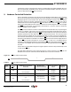
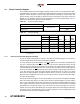
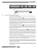
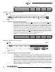
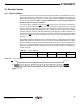
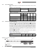
Table Of Contents
- Features
- 1. Description
- 2. Pin Configurations and Pinouts
- 3. Block Diagram
- 4. Memory Array
- 5. Device Operation
- 6. Read Commands
- 7. Program and Erase Commands
- 8. Sector Protection
- 9. Hardware Controlled Protection
- 10. Security Features
- 11. Additional Commands
- 12. Deep Power-down
- 13. “Power of 2” Binary Page Size Option
- 14. Manufacturer and Device ID Read
- 15. Command Tables
- 16. Power-on/Reset State
- 17. System Considerations
- 18. Electrical Specifications
- 19. Input Test Waveforms and Measurement Levels
- 20. Output Test Load
- 21. AC Waveforms
- 21.1 Waveform 1 – SPI Mode 0 Compatible (for Frequencies up to 66MHz)
- 21.2 Waveform 2 – SPI Mode 3 Compatible (for Frequencies up to 66MHz)
- 21.3 Waveform 3 – RapidS Mode 0 (FMAX = 66MHz)
- 21.4 Waveform 4 – RapidS Mode 3 (FMAX = 66MHz)
- 21.5 Utilizing the RapidS Function
- 21.6 Reset Timing
- 21.7 Command Sequence for Read/Write Operations for Page Size 256-Bytes (Except Status Register Read, Manufacturer and Device ID Read)
- 21.8 Command Sequence for Read/Write Operations for Page Size 264-Bytes (Except Status Register Read, Manufacturer and Device ID Read)
- 22. Write Operations
- 23. Read Operations
- 24. Detailed Bit-level Read Waveform – RapidS Serial Interface Mode 0/Mode 3
- 24.1 Continuous Array Read (Legacy Opcode E8H)
- 24.2 Continuous Array Read (Opcode 0BH)
- 24.3 Continuous Array Read (Low Frequency: Opcode 03H)
- 24.4 Main Memory Page Read (Opcode: D2H)
- 24.5 Buffer Read (Opcode D4H or D6H)
- 24.6 Buffer Read (Low Frequency: Opcode D1H or D3H)
- 24.7 Read Sector Protection Register (Opcode 32H)
- 24.8 Read Sector Lockdown Register (Opcode 35H)
- 24.9 Read Security Register (Opcode 77H)
- 24.10 Status Register Read (Opcode D7H)
- 24.11 Manufacturer and Device Read (Opcode 9FH)
- 25. Auto Page Rewrite Flowchart
- 26. Ordering Information
- 27. Packaging Information
- 28. Revision History
- 29. Errata
16
3596N–DFLASH–11/2012
AT45DB081D
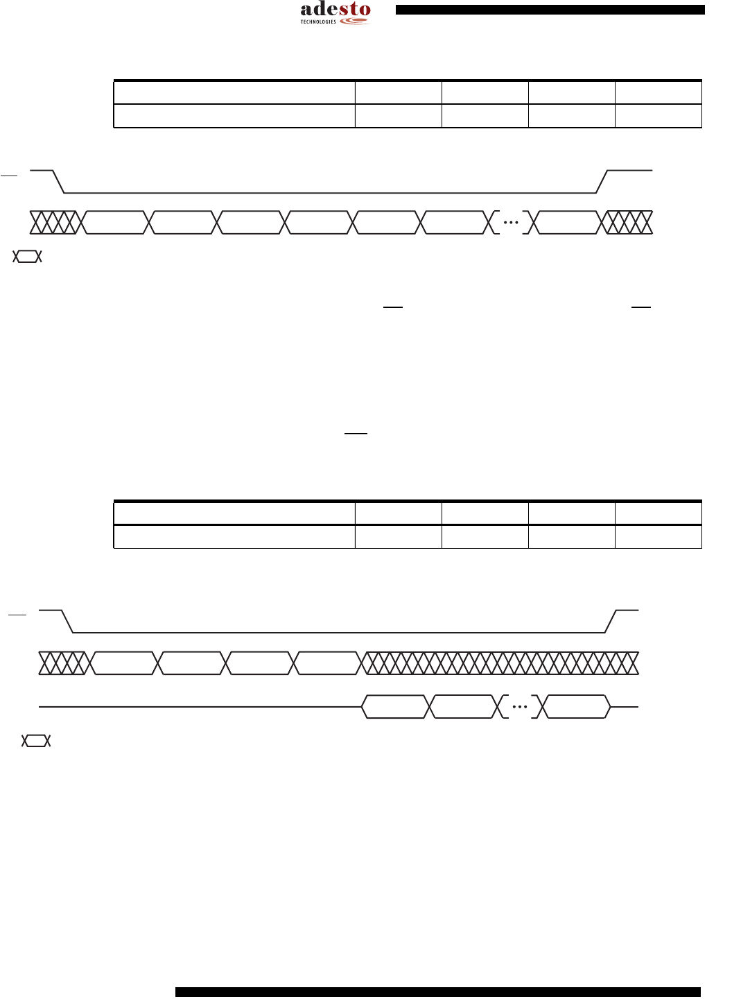
Table 9-5. Program Sector Protection Register Command
Figure 9-3. Program Sector Protection Register
9.1.3 Read Sector Protection Register Command
To read the Sector Protection Register, the
CS pin must first be asserted. Once the CS pin has
been asserted, an opcode of 32H and three dummy bytes must be clocked in via the SI pin. After
the last bit of the opcode and dummy bytes have been clocked in, any additional clock pulses on
the SCK pins will result in data for the content of the Sector Protection Register being output on
the SO pin. The first byte corresponds to sector 0 (0a, 0b), the second byte corresponds to sec-
tor one and the last byte (byte 16) corresponds to sector 15. Once the last byte of the Sector
Protection Register has been clocked out, any additional clock pulses will result in undefined
data being output on the SO pin. The
CS must be deasserted to terminate the Read Sector Pro-
tection Register operation and put the output into a high-impedance state.
Table 9-6. Read Sector Protection Register Command
Note: xx = Dummy Byte
Figure 9-4. Read Sector Protection Register
9.1.4 Various Aspects About the Sector Protection Register
The Sector Protection Register is subject to a limit of 10,000 erase/program cycles. Users are
encouraged to carefully evaluate the number of times the Sector Protection Register will be
modified during the course of the applications’ life cycle. If the application requires that the Sec-
tor Protection Register be modified more than the specified limit of 10,000 cycles because the
application needs to temporarily unprotect individual sectors (sector protection remains enabled
while the Sector Protection Register is reprogrammed), then the application will need to limit this
practice. Instead, a combination of temporarily unprotecting individual sectors along with dis-
abling sector protection completely will need to be implemented by the application to ensure that
the limit of 10,000 cycles is not exceeded.
Command Byte 1 Byte 2 Byte 3 Byte 4
Program Sector Protection Register 3DH 2AH 7FH FCH
Data Byte
n
Opcode
Byte 1
Opcode
Byte 2
Opcode
Byte 3
Opcode
Byte 4
Data Byte
n + 1
Data Byte
n + 15
CS
Each transition
represents 8 bits
SI
Command Byte 1 Byte 2 Byte 3 Byte 4
Read Sector Protection Register 32H xxH xxH xxH
Opcode X X X
Data Byte
n
Data Byte
n + 1
CS
Data Byte
n + 15
SI
SO
Each transition
represents 8 bits