
User guide
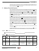
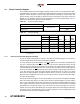
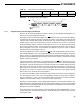
Table Of Contents
- Features
- 1. Description
- 2. Pin Configurations and Pinouts
- 3. Block Diagram
- 4. Memory Array
- 5. Device Operation
- 6. Read Commands
- 7. Program and Erase Commands
- 8. Sector Protection
- 9. Hardware Controlled Protection
- 10. Security Features
- 11. Additional Commands
- 12. Deep Power-down
- 13. “Power of 2” Binary Page Size Option
- 14. Manufacturer and Device ID Read
- 15. Command Tables
- 16. Power-on/Reset State
- 17. System Considerations
- 18. Electrical Specifications
- 19. Input Test Waveforms and Measurement Levels
- 20. Output Test Load
- 21. AC Waveforms
- 21.1 Waveform 1 – SPI Mode 0 Compatible (for Frequencies up to 66MHz)
- 21.2 Waveform 2 – SPI Mode 3 Compatible (for Frequencies up to 66MHz)
- 21.3 Waveform 3 – RapidS Mode 0 (FMAX = 66MHz)
- 21.4 Waveform 4 – RapidS Mode 3 (FMAX = 66MHz)
- 21.5 Utilizing the RapidS Function
- 21.6 Reset Timing
- 21.7 Command Sequence for Read/Write Operations for Page Size 256-Bytes (Except Status Register Read, Manufacturer and Device ID Read)
- 21.8 Command Sequence for Read/Write Operations for Page Size 264-Bytes (Except Status Register Read, Manufacturer and Device ID Read)
- 22. Write Operations
- 23. Read Operations
- 24. Detailed Bit-level Read Waveform – RapidS Serial Interface Mode 0/Mode 3
- 24.1 Continuous Array Read (Legacy Opcode E8H)
- 24.2 Continuous Array Read (Opcode 0BH)
- 24.3 Continuous Array Read (Low Frequency: Opcode 03H)
- 24.4 Main Memory Page Read (Opcode: D2H)
- 24.5 Buffer Read (Opcode D4H or D6H)
- 24.6 Buffer Read (Low Frequency: Opcode D1H or D3H)
- 24.7 Read Sector Protection Register (Opcode 32H)
- 24.8 Read Sector Lockdown Register (Opcode 35H)
- 24.9 Read Security Register (Opcode 77H)
- 24.10 Status Register Read (Opcode D7H)
- 24.11 Manufacturer and Device Read (Opcode 9FH)
- 25. Auto Page Rewrite Flowchart
- 26. Ordering Information
- 27. Packaging Information
- 28. Revision History
- 29. Errata
15
3596N–DFLASH–11/2012
AT45DB081D
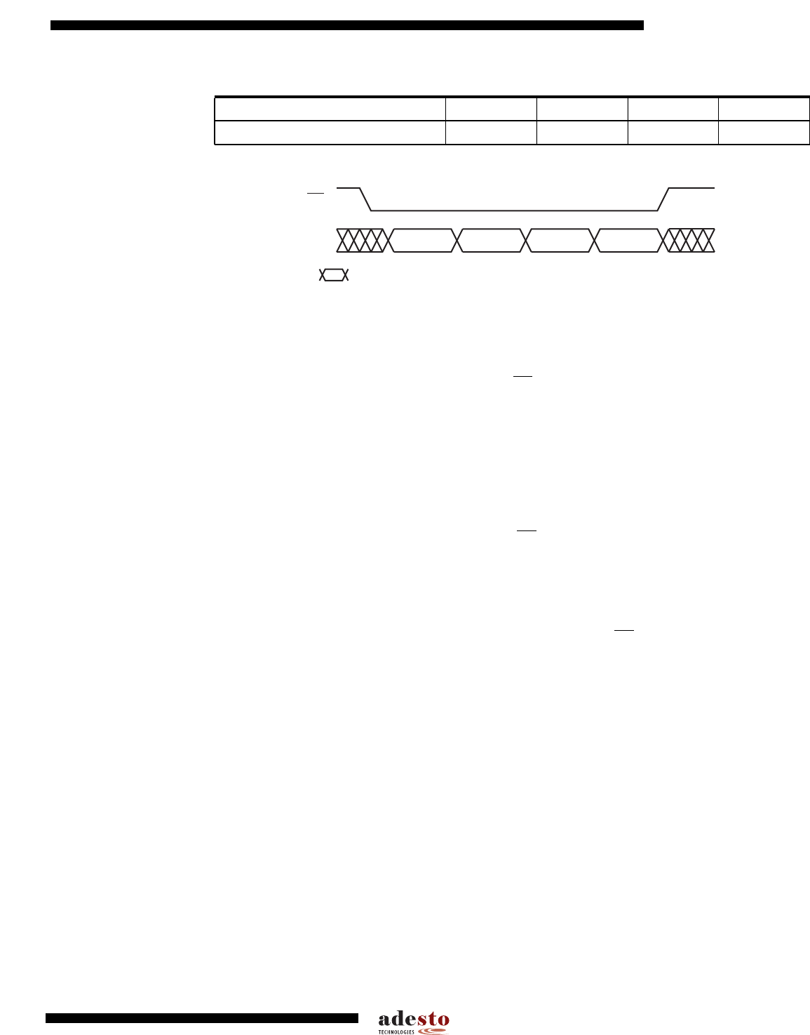
Table 9-4. Erase Sector Protection Register Command
Figure 9-2. Erase Sector Protection Register
9.1.2 Program Sector Protection Register Command
Once the Sector Protection Register has been erased, it can be reprogrammed using the Pro-
gram Sector Protection Register command.
To program the Sector Protection Register, the CS pin must first be asserted and the appropri-
ate 4-byte opcode sequence must be clocked into the device via the SI pin. The 4-byte opcode
sequence must start with 3DH and be followed by 2AH, 7FH, and FCH. After the last bit of the
opcode sequence has been clocked into the device, the data for the contents of the Sector
Protection Register must be clocked in. As described in Section 9.1, the Sector Protection Reg-
ister contains 16-bytes of data, so 16-bytes must be clocked into the device. The first byte of
data corresponds to sector zero, the second byte corresponds to sector one, and so on with the
last byte of data corresponding to sector 15.
After the last data byte has been clocked in, the CS pin must be deasserted to initiate the inter-
nally self-timed program cycle. The programming of the Sector Protection Register should take
place in a time of t
P
, during which time the Status Register will indicate that the device is busy. If
the device is powered-down during the program cycle, then the contents of the Sector Protection
Register cannot be guaranteed.
If the proper number of data bytes is not clocked in before the CS pin is deasserted, then the
protection status of the sectors corresponding to the bytes not clocked in can not be guaranteed.
For example, if only the first two bytes are clocked in instead of the complete 16-bytes, then the
protection status of the last 14 sectors cannot be guaranteed. Furthermore, if more than 16-
bytes of data is clocked into the device, then the data will wrap back around to the beginning of
the register. For instance, if 17-bytes of data are clocked in, then the 17
th
byte will be stored at
byte location zero of the Sector Protection Register.
If a value other than 00H or FFH is clocked into a byte location of the Sector Protection Register,
then the protection status of the sector corresponding to that byte location cannot be guaran-
teed. For example, if a value of 17H is clocked into byte location two of the Sector Protection
Register, then the protection status of sector two cannot be guaranteed.
The Sector Protection Register can be reprogrammed while the sector protection enabled or dis-
abled. Being able to reprogram the Sector Protection Register with the sector protection enabled
allows the user to temporarily disable the sector protection to an individual sector rather than dis-
abling sector protection completely.
The Program Sector Protection Register command utilizes the internal SRAM buffer 1 for pro-
cessing. Therefore, the contents of the buffer 1 will be altered from its previous state when this
command is issued.
Command Byte 1 Byte 2 Byte 3 Byte 4
Erase Sector Protection Register 3DH 2AH 7FH CFH
Opcode
Byte 1
Opcode
Byte 2
Opcode
Byte 3
Opcode
Byte 4
CS
Each transition
represents 8 bits
SI