
Manual


51
3595R–DFLASH–11/2012
AT45DB041D
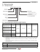
28. Revision History
Revision Level – Revision Date History
A – October 2005 Initial Release
B – March 2006
Added “Preliminary”.
Added text, in “Programming the Configuration Register”, to
indicate that power cycling is required to switch to “power of 2” page
size after the opcode enable has been executed.
Added “Legacy Commands” table.
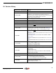
C – June 2006 Corrected typographical errors.
D – July 2006 Corrected typographical errors.
E – August 2006 Added errata regarding Chip Erase.
F – November 2006 Removed “Preliminary”.
G – February 2007 Removed RDY/
BUSY pin references.
H – March 2007
Changed page size description from 512 to 256 in Table 15-6.
Changed page size description from 528 to 264 in Table 15-7.
Added additional text for “power of 2” binary page size option.
I – April 2007
Removed SER/
BYTE statement from SI and SO pin descriptions in
Table 2-1.
Changed the number of don’t care bits from 17 to 16 for sector 1-15
erase in Section 7.6.
Corrected the density code description from 16-Mbit to 4-Mbit in
Section 14.1.2.
Changed A16 address bit for opcode 7Ch from “x” to “A” in Table
15-6.
Chagned PA8 address bit for opcode 7Ch from “x” to “P” in Table
15-7.
J – August 2007
Changed t
XFR
and t
COMP
values from 40 µs to 200µs.
Changed t
VCSL
from 50µs to 70µs.
Changed t
RDPD
from 30µs to 35µs.
K – December 2007 Changed Note 1 on page 14 from “0 through 15” to “0 through 7”.
L – April 2008
The Chip Erase command is supported on devices with date code
0810 and later.
Added Chip Erase time.
Added part nuber ordering code details for suffixes SL954/955.
Added ordering code detail.
M – February 2009 Changed t
DIS
(Typ and Max) to 27ns and 35ns, respectively.
N – March 2009
Changed Deep Power-Down Current values
- Increased typical value from 5µA to 15µA.
- Increased maximum value from 15µA to 25µA.
O – April 2009
Updated Absolute Maximum Ratings
Removed Chip Erase Errata