
Owner manual


53
AT45DB021E [PRELIMINARY DATASHEET]
8789B–DFLASH–11/2012
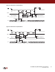
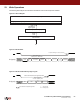
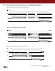
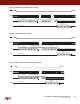
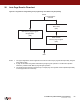
24. Read Operations
The following block diagram and waveforms illustrate the various read sequences available.
Figure 24-1. Block Diagram
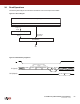
Figure 24-2. Main Memory Page Read
Flash Memory Array
Page (256/264 bytes)
Buffer (256/264 bytes)
I/O Interface
Main Memory
Page To
Buffer
Main Memory
Page Read
Buffer
Read
SO
CS
SI (Input)
SO (Output)
n
CMD PA8-7 PA6-0, BA8 BA7-0 X X
Address for Binary Page Size
A16 A15-A8 A7-A0
n n + 1
4 Dummy Bytes