
Owner manual


46
AT45DB021E [PRELIMINARY DATASHEET]
8789B–DFLASH–11/2012
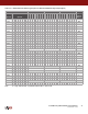
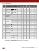
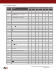
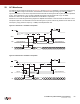
18.4 AC Characteristics
Note: 1. Values are based on device characterization, not 100% tested in production.
Symbol Parameter
1.65V to 3.6V 2.3V to 3.6V
Min Typ Max Min Typ Max Units
f
SCK
SCK Frequency 70 70 MHz
f
CAR1
SCK Frequency for Continuous Read 70 70 MHz
f
CAR2
SCK Frequency for Continuous Read
(Low Frequency)
33 33 MHz
f
CAR3
SCK Frequency for Continuous Read
(Low Power Mode – 01h Opcode)
20 20 MHz
t
WH
SCK High Time 6.4 6.4 ns
t
WL
SCK Low Time 6.4 6.4 ns
t
SCKR
(1)
SCK Rise Time, Peak-to-peak 0.1 0.1 V/ns
t
SCKF
(1)
SCK Fall Time, Peak-to-peak 0.1 0.1 V/ns
t
CS
Minimum CS High Time 30 30 ns
t
CSS
CS Setup Time 6 5 ns
t
CSH
CS Hold Time 5 5 ns
t
SU
Data In Setup Time 2 2 ns
t
H
Data In Hold Time 1 1 ns
t
HO
Output Hold Time 0 0 ns
t
DIS
Output Disable Time 8 6 ns
t
V
Output Valid 8 6 ns
t
WPE
WP Low to Protection Enabled 1 1 μs
t
WPD
WP High to Protection Disabled 1 1 μs
t
LOCK
Freeze Sector Lockdown Time
(from
CS High)
200 200 μs
t
EUDPD
CS High to Ultra-Deep Power-Down 3 3 μs
t
CSLU
Minimum CS Low Time to Exit Ultra-Deep
Power-Down
20 20 ns
t
XUDPD
Exit Ultra-Deep Power-Down Time 240 120 μs
t
EDPD
CS High to Deep Power-Down 3 3 μs
t
RDPD
Resume from Deep Power-Down Time 35 35 μs
t
XFR
Page to Buffer Transfer Time 100 85 μs
t
COMP
Page to Buffer Compare Time 100 85 μs
t
RST
RESET Pulse Width 10 10 μs
t
REC
RESET Recovery Time 1 1 μs
t
SWRST
Software Reset Time 30 30 μs