
Owner manual

14
AT45DB021E [PRELIMINARY DATASHEET]
8789B–DFLASH–11/2012
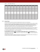
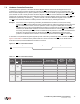
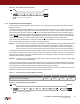
Table 6-2. Sector Erase Addressing
6.9 Chip Erase
The Chip Erase command allows the entire main memory array to be erased at one time.
To execute the Chip Erase command, a 4-byte command sequence of C7h, 94h, 80h, and 9Ah must be clocked into the
device. Since the entire memory array is to be erased, no address bytes need to be clocked into the device and any data
clocked in after the opcode will be ignored. After the last bit of the opcode sequence has been clocked in, the
CS pin
must be deasserted to start the erase process. The erase operation is internally self-timed and should take place in a
time of t
CE
. During this time, the RDY/BUSY bit in the Status Register will indicate that the device is busy.
The Chip Erase command will not affect sectors that are protected or locked down; the contents of those sectors will
remain unchanged. Only those sectors that are not protected or locked down will be erased.
The
WP pin can be asserted while the device is erasing, but protection will not be activated until the internal erase cycle
completes.
The device also incorporates an intelligent erase algorithm that can detect when a byte location fails to erase properly. If
an erase error arises, it will be indicated by the EPE bit in the Status Register.
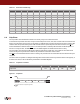
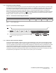
Table 6-3. Chip Erase Command
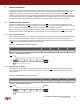
Figure 6-1. Chip Erase
PA9/A17 PA8/A16 PA7/A15 PA6/A14 PA5/A13 PA4/A12 PA3/A11 PA2/A10 PA1/A9 PA0/A8 Sector
0 0 0 0 0 0 0 X X X 0a
0 0 0 0 0 0 1 X X X 0b
0 0 1 X X X X X X X 1
•
•
•
•
•
•
•
•
•
•
•
•
•
•
•
•
•
•
•
•
•
•
•
•
•
•
•
•
•
•
•
•
•
1 0 1 X X X X X X X 5
1 1 0 X X X X X X X 6
1 1 1 X X X X X X X 7
Command Byte 1 Byte 2 Byte 3 Byte 4
Chip Erase C7h 94h 80h 9Ah
C7h 94h 80h 9Ah
CS
Each transition represents eight bits