
Owner manual


47
3638K–DFLASH–11/2012
AT45DB021D
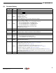
23. Revision History
Doc. Rev. Date Comments
A 06/2006 Initial release.
B 02/2007 Removed RDY/
BUSY pin references.
C 08/2007
Changed t
VCSL
time to 1ms
Changed I
DP
(Max) to 15µA
Added Chip Erase time
Changed t
RDPD
time to 35µs
Fixed the typographical error in the Block Architecture diagram
D 11/2007
Changed the t
XFR
and t
COMP
times from 400µs to 200µs
Changed part number ordering code to reflect NiPdAu lead finish
- Changed AT45DB021D-MU to AT45DB021D-MH
- Changed AT45DB021D-SSU to AT45DB021D-SSH
- Changed AT45DB021D-SU to AT45DB021D-SH
Added lead finish details to Ordering Information table
Added Ordering Code Detail
E 02/2008 Fixed the typographical error, under Status Register Read, to indicate that bit 3 is a “0”
F 04/2008
Replaced 8M1-A MLF Package with 8MA1 UDFN Package
Added part number ordering code details for suffixes SL954/955
G 02/2009 Changed t
DIS
(Typ and Max) to 27ns and 35ns, respectively
H 03/2009
Changed Deep Power-Down Current values
- Increased typical value from 5µA to 15µA
- Increased maximum value from 15µA to 25µA
I 04/2009
Updated Absolute Maximum Ratings
Updated System Specifications
J 05/2010
Updated template
Changed number of bytes and sectors in Section 7.1.2 on page 13
Changed T
SE
values in Table 16-3 on page 31
- Typ from 0.8 to 400, Max from 2.5 to 700 and Units from s to ms
Changed BA0 to PA0 and x to P under PA3, row 50h in Table 13-7 on page 27
Changed A11 from x to P, row 50h in Table 13-6 on page 26
Changed from 10,000 to 20,000 cumulative page erase/program operations in Section 9.3
Added “Please contact Adesto for availability of devices that are specified to exceed the 20K
cycle cumulative limit” in Section 9.3
K 11/2012 Update to Adesto Logos