
Owner's manual


32
3639J–DFLASH–11/2012
AT45DB011D
18. Electrical Specifications
Notes: 1. I
CC1
during a buffer read is 20mA maximum @ 20MHz
2. All inputs (SI, SCK,
CS, WP, and RESET) are guaranteed by design to be 5-Volt tolerant
Table 18-1. Absolute Maximum Ratings*
Temperature under Bias ................................. -55C to +125C
*NOTICE: Stresses beyond those listed under “Absolute
Maximum Ratings” may cause permanent dam-
age to the device. The "Absolute Maximum Rat-
ings" are stress ratings only and functional
operation of the device at these or any other con-
ditions beyond those indicated in the operational
sections of this specification is not implied. Expo-
sure to absolute maximum rating conditions for
extended periods may affect device reliability.
Voltage Extremes referenced in the "Absolute
Maximum Ratings" are intended to accommo-
date short duration undershoot/overshoot condi-
tions and does not imply or guarantee functional
device operation at these levels for any extended
period of time
Storage Temperature...................................... -65C to +150C
All Input Voltages (except V
CC
but including NC Pins)
with Respect to Ground ...................................-0.6V to +6.25V
All Output Voltages
with Respect to Ground .............................-0.6V to V
CC
+ 0.6V
Table 18-2. DC and AC Operating Range
AT45DB011D
Operating Temperature (Case) Ind. -40Cto85C
V
CC
Power Supply 2.7V to 3.6V
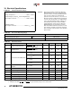
Table 18-3. DC Characteristics
Symbol Parameter Condition Min Typ Max Units
I
DP
Deep Power-down Current
CS, RESET, WP = V
IH
,all
inputs at CMOS levels
15 25 µA
I
SB
Standby Current
CS, RESET, WP = V
IH
,all
inputs at CMOS levels
25 50 µA
I
CC1
(1)
Active Current, Read Operation
f = 20MHz; I
OUT
= 0mA;
V
CC
= 3.6V
710mA
f = 33MHz; I
OUT
= 0mA;
V
CC
= 3.6V
812mA
f = 50MHz; I
OUT
= 0mA;
V
CC
= 3.6V
10 14 mA
f = 66MHz; I
OUT
= 0mA;
V
CC
= 3.6V
15 25 mA
I
CC2
Active Current, Program/Erase
Operation
V
CC
= 3.6V 12 20 mA
I
LI
Input Load Current V
IN
= CMOS levels 1 µA
I
LO
Output Leakage Current V
I/O
= CMOS levels 1 µA
V
IL
Input Low Voltage V
CC
x 0.3 V
V
IH
Input High Voltage V
CC
x 0.7 V
V
OL
Output Low Voltage I
OL
= 1.6mA; V
CC
= 2.7V 0.4 V
V
OH
Output High Voltage I
OH
= -100µA V
CC
-0.2V V