
User Manual


38
9570H–AT42–02/10
AT42QT1110-MZ/AT42QT1110-AZ
8. Specifications
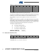
8.1 Absolute Maximum Specifications
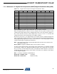
8.2 Recommended Operating Conditions
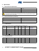
8.3 DC Specifications
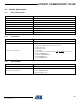
8.4 Timing Specifications
Vdd -0.5 to +6V
Max continuous pin current, any control or drive pin ±10 mA
Voltage forced onto any pin -1.0V to (Vdd + 0.5) Volts
EEPROM setups maximum writes 100,000 write cycles
CAUTION: Stresses beyond those listed under Absolute Maximum Specifications may cause permanent damage to the
device. This is a stress rating only and functional operation of the device at these or other conditions beyond those indicated
in the operational sections of this specification is not implied. Exposure to absolute maximum specification conditions for
extended periods may affect device reliability
Operating temperature -40°C to +125°C
Storage temperature -65°C to +150°C
Vdd 3V to 5.5V
Supply ripple + noise ±20 mV
Cx transverse load capacitance per key 2 to 20 pF
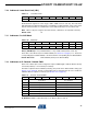
Vdd = 5.0V, Cs = 4.7 nF, Rs = 1 M, Ta = recommended range, unless otherwise noted
Parameter Description Min Typ Max Units Notes
Iddr Average supply current, running – –
12 at 5V
8 at 3V
mA
For typical values
seeSection 8.8
Vil Low input logic level -0.5V – 0.3 Vdd V
Vih High input logic level 0.6 Vdd Vdd Vdd + 0.5V V
Vol Low output voltage 0 – 0.7 V 10 mA sink current
Voh High output voltage 0.8 Vdd – Vdd V 10 mA source current
Iil Input leakage current – <0.05 1 µA
Rrst Internal RST
pull-up resistor 30 – 60 k
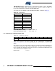
Parameter Description Min Typ Max Units Notes
T
BS Burst duration – 5 – ms 4.7 nF Cs
Fc Burst center frequency – 53 – kHz
Fm Burst modulation, percentage – 18 – %
T
PW Pulse width – 6000 – ns