
Owner manual


5
AT29LV512
0177M–05/02
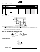
Notes: 1. After power is applied and V
CC
is at the minimum specified data sheet value, the system should wait 20 ms before an
operational mode is started.
Notes: 1. X can be V
IL
or V
IH
.
2. Refer to AC Programming Waveforms.
3. V
H
= 12.0V ± 0.5V.
4. Manufacturer Code is 1F. The Device Code is 3D.
5. See details under Software Product Identification Entry/Exit.
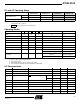
DC and AC Operating Range
AT29LV512-12 AT29LV512-15 AT29LV512-20 AT29LV512-25
Operating
Temperature (Case)
Com. 0°C-70°C0°C-70°C
0°C-70°C 0°C-70°C
Ind. -40°C-85°C-40°C-85°C
-40°C-85°C -40°C-85°C
V
CC
Power Supply
(1)
3.3V ± 0.3V 3.3V ± 0.3V 3.3V ± 0.3V 3.3V ± 0.3V
2.
Not recommended for New Designs.
Operating Modes
Mode CE OE WE Ai I/O
Read V
IL
V
IL
V
IH
Ai D
OUT
Program
(2)
V
IL
V
IH
V
IL
Ai D
IN
Standby/Write Inhibit V
IH
X
(1)
XXHighZ
Program Inhibit X X V
IH
Program Inhibit X V
IL
X
Output Disable X V
IH
XHighZ
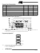
Product Identification
Hardware V
IL
V
IL
V
IH
A1 - A15 = V
IL
,A9=V
H
(3)
,A0=V
IL
Manufacturer Code
(4)
A1 - A15 = V
IL
,A9=V
H
(3)
,A0=V
IH
Device Code
(4)
Software
(5)
A0 = V
IL
Manufacturer Code
(4)
A0 = V
IH
Device Code
(4)
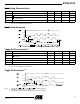
DC Characteristics
Symbol Parameter Condition Min Max Units
I
LI
Input Load Current V
IN
=0VtoV
CC
1µA
I
LO
Output Leakage Current V
I/O
=0VtoV
CC
1µA
I
SB1
V
CC
Standby Current CMOS CE =V
CC
-0.3VtoV
CC
Com. 40 µA
Ind. 50 µA
I
SB2
V
CC
Standby Current TTL CE =2.0VtoV
CC
1mA
I
CC
V
CC
Active Current f = 5 MHz; I
OUT
=0mA;V
CC
=3.6V 15 mA
V
IL
Input Low Voltage 0.6 V
V
IH
Input High Voltage 2.0 V
V
OL
Output Low Voltage I
OL
=1.6mA;V
CC
=3.0V 0.45 V
V
OH
Output High Voltage I
OH
=-100µA;V
CC
=3.0V 2.4 V