
User Manual
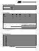

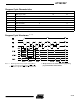


AC Read Characteristics
AT29C257-70 AT29C257-90 AT29C257-12 AT29C257-15
Symbol Parameter
Min Max Min Max Min Max Min Max
Units
t
ACC
Address to Output Delay 70 90 120 150 ns
t
CE
(1)
CE to Output Delay 70 90 120 150 ns
t
OE
(2)
OE to Output Delay 0 40 0 40 0 50 0 70 ns
t
DF
(3, 4)
CE or OE to Output Float 0 25 0 25 0 30 0 40 ns
t
OH
Output Hold from OE, CE
or Address, whichever
occurred first
0000 ns
Notes: 1. CE may be delayed up to t
ACC
- t
CE
after the address
transition without impact on t
ACC
.
2.
OE may be delayed up to t
CE
- t
OE
after the falling
edge of
CE without impact on t
CE
or by t
ACC
- t
OE
after an address change without impact on t
ACC
.
3. t
DF
is specified from OE or CE whichever occurs first
(C
L
= 5 pF).
4. This parameter is characterized and is not 100% tested.
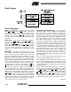
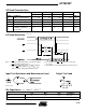
AC Read Waveforms
(1, 2, 3, 4)
t
R
, t
F
< 5 ns
Input Test Waveforms and Measurement Level
Output Test Load
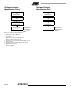
Pin Capacitance
(f = 1 MHz, T = 25°C)
(1)
Typ Max Units Conditions
C
IN
46pFV
IN
= 0V
C
OUT
812pFV
OUT
= 0V
Note: 1. This parameter is characterized and is not 100% tested.
AT29C257
4-109