
Manual

6
AT29BV040A
0383F–FLASH–05/02
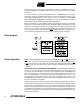
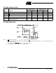
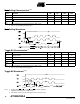
AC Read Waveforms
Notes: 1. CE may be delayed up to t
ACC
-t
CE
after the address transition without impact on t
ACC
.
6. OE
may be delayed up to t
CE
-t
OE
after the falling edge of CE without impact on t
CE
or by t
ACC
-t
OE
after an address change
without impact on t
ACC
.
7. t
DF
is specified from OE or CE whichever occurs first (CL = 5 pF).
8. This parameter is characterized and is not 100% tested.
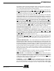
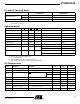
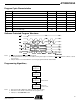
AC Read Characteristics
Symbol Parameter
AT29BV040A-20 AT29BV040A-25
UnitsMin Max Min Max
t
ACC
Address to Output Delay 200 250 ns
t
CE
(1)
CE to Output Delay 200 250 ns
t
OE
(6)
OE to Output Delay 0 80 0 120 ns
t
DF
(7)(8)
CE or OE to Output Float 0 50 0 60 ns
t
OH
Output Hold from OE,CEor Address,
whichever occurred first
00ns