
Owner's manual
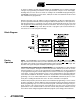
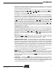
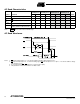
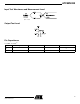
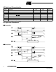
Table Of Contents
- Features
- Description
- Pin Configurations
- Block Diagram
- Device Operation
- Absolute Maximum Ratings*
- DC and AC Operating Range
- Operating Modes
- DC Characteristics
- AC Read Characteristics
- AC Read Waveforms
- Input Test Waveforms and Measurement Level
- Output Test Load
- Pin Capacitance
- AC Byte Load Characteristics
- AC Byte Load Waveforms(1)(2)
- Program Cycle Characteristics
- Software Protected Program Waveform
- Programming Algorithm(1)
- Data Polling Characteristics(1)(2)
- Data Polling Waveforms
- Toggle Bit Characteristics(1)
- Toggle Bit Waveforms(1)(3)
- Software Product Identification Entry(1)
- Software Product Identification Exit(1)
- Boot Block Lockout Feature Enable Algorithm(1)
- Ordering Information
- Packaging Information
9
AT29BV020
0402D–FLASH–05/02
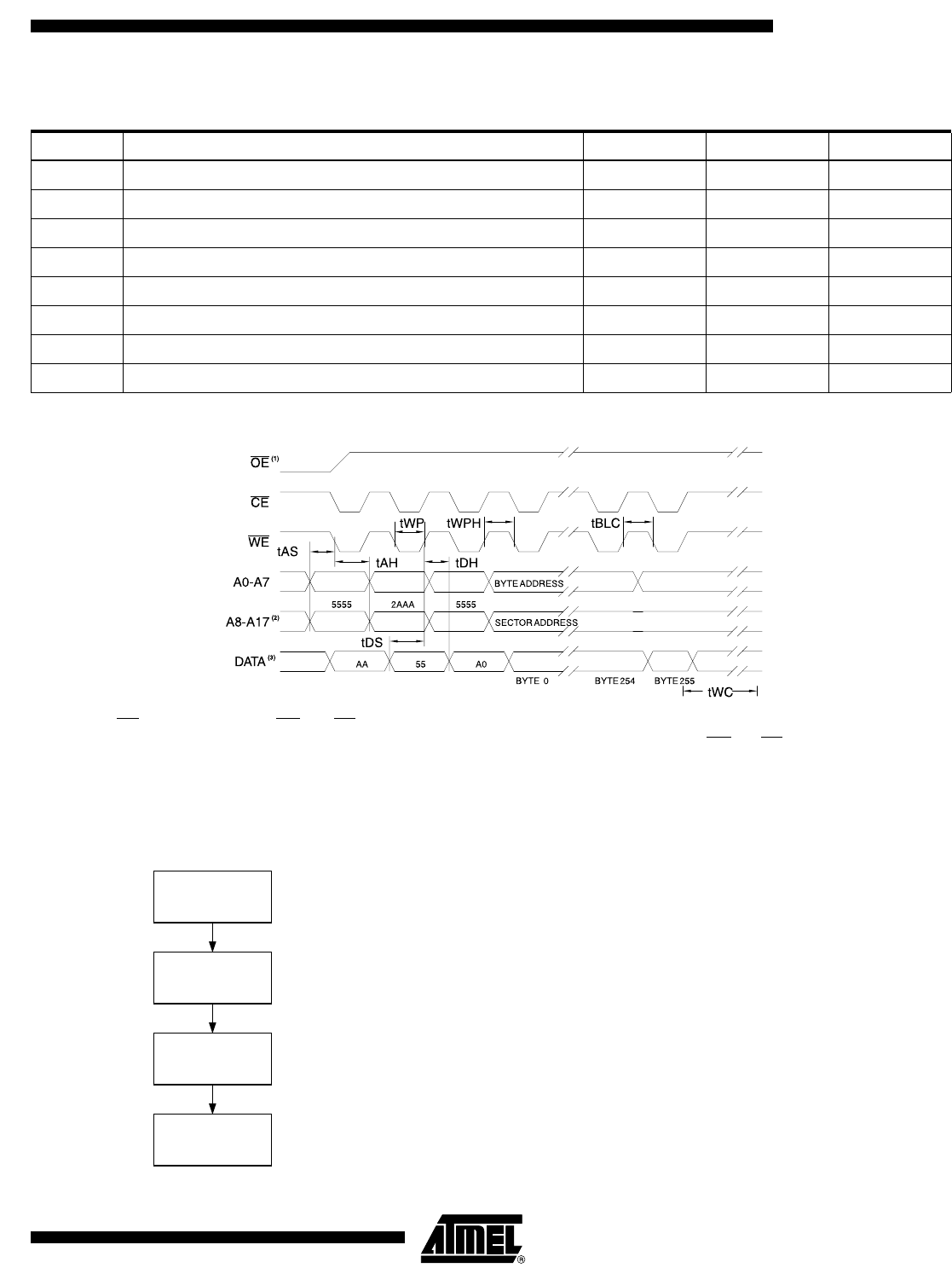
Software Protected Program Waveform
Notes: 1. OE must be high when WE and CE are both low.
2. A8 through A17 must specify the sector address during each high-to-low transition of WE
(or CE) after the software code
has been entered.
3. Data in bytes not loaded within a sector being programmed may be altered by the program operation; therefore, all bytes
within a sector must be loaded.
Programming Algorithm
(1)
Program Cycle Characteristics
Symbol Parameter Min Max Units
t
WC
WriteCycleTime 20 ms
t
AS
Address Set-up Time 10 ns
t
AH
Address Hold Time 100 ns
t
DS
Data Set-up Time 100 ns
t
DH
Data Hold Time 10 ns
t
WP
Write Pulse Width 200 ns
t
BLC
Byte Load Cycle Time 150 µs
t
WPH
Write Pulse Width High 200 ns
LOAD DATA AA
TO
ADDRESS 5555
LOAD DATA 55
TO
ADDRESS 2AAA
LOAD DATA A0
TO
ADDRESS 5555
LOAD DATA
TO
SECTOR (256 BYTES)
(3)
WRITES ENABLED
ENTER DATA
PROTECT STATE
(2)
Notes: 1. Data Format: I/O7 - I/O0 (Hex);
Address Format: A14 - A0 (Hex).
2. Data Protect state will be re-activated at end of
program cycle.
3. 256 bytes of data MUST BE loaded.