
Owner's manual
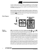
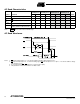
Table Of Contents
- Features
- Description
- Pin Configurations
- Block Diagram
- Device Operation
- Absolute Maximum Ratings*
- DC and AC Operating Range
- Operating Modes
- DC Characteristics
- AC Read Characteristics
- AC Read Waveforms
- Input Test Waveforms and Measurement Level
- Output Test Load
- Pin Capacitance
- AC Byte Load Characteristics
- AC Byte Load Waveforms(1)(2)
- Program Cycle Characteristics
- Software Protected Program Waveform
- Programming Algorithm(1)
- Data Polling Characteristics(1)(2)
- Data Polling Waveforms
- Toggle Bit Characteristics(1)
- Toggle Bit Waveforms(1)(3)
- Software Product Identification Entry(1)
- Software Product Identification Exit(1)
- Boot Block Lockout Feature Enable Algorithm(1)
- Ordering Information
- Packaging Information
8
AT29BV020
0402D–FLASH–05/02
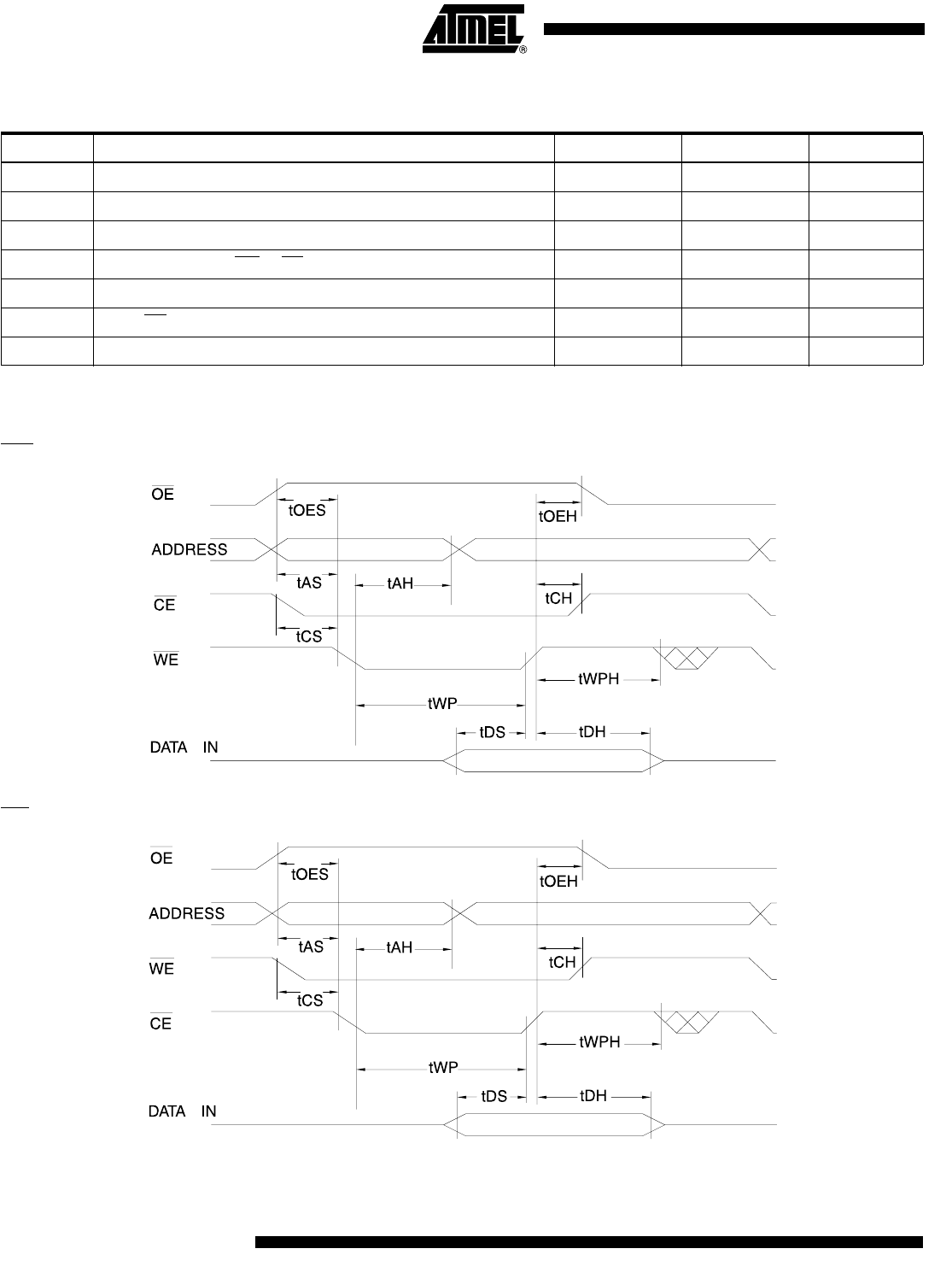
AC Byte Load Waveforms
(1)(2)
WE Controlled
CE
Controlled
AC Byte Load Characteristics
Symbol Parameter Min Max Units
t
AH
Address Hold Time 100 ns
t
CS
Chip Select Set-up Time 0 ns
t
CH
Chip Select Hold Time 0 ns
t
WP
Write Pulse Width (WE or CE) 200 ns
t
DS
Data Set-up Time 100 ns
t
DH
,t
OEH
Data, OE Hold Time 10 ns
t
WPH
Write Pulse Width High 200 ns