
Owner's manual
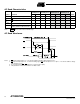
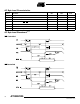
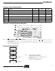
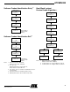

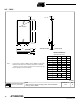
Table Of Contents
- Features
- Description
- Pin Configurations
- Block Diagram
- Device Operation
- Absolute Maximum Ratings*
- DC and AC Operating Range
- Operating Modes
- DC Characteristics
- AC Read Characteristics
- AC Read Waveforms
- Input Test Waveforms and Measurement Level
- Output Test Load
- Pin Capacitance
- AC Byte Load Characteristics
- AC Byte Load Waveforms(1)(2)
- Program Cycle Characteristics
- Software Protected Program Waveform
- Programming Algorithm(1)
- Data Polling Characteristics(1)(2)
- Data Polling Waveforms
- Toggle Bit Characteristics(1)
- Toggle Bit Waveforms(1)(3)
- Software Product Identification Entry(1)
- Software Product Identification Exit(1)
- Boot Block Lockout Feature Enable Algorithm(1)
- Ordering Information
- Packaging Information
13
AT29BV020
0402D–FLASH–05/02
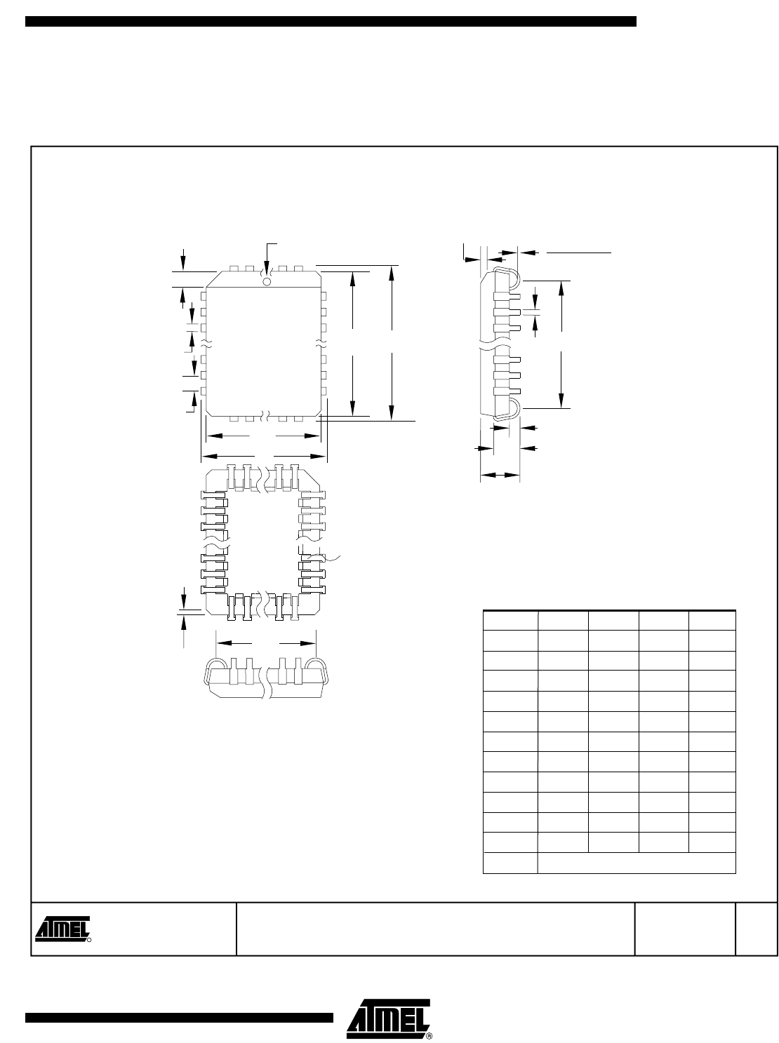
Packaging Information
32J–PLCC
DRAWING NO.
REV.
2325 Orchard Parkway
San Jose, CA 95131
R
TITLE
32J, 32-lead, Plastic J-leaded Chip Carrier (PLCC)
B
32J
10/04/01
1.14(0.045) X 45˚
PIN NO. 1
IDENTIFIER
1.14(0.045) X 45˚
0.51(0.020)MAX
0.318(0.0125)
0.191(0.0075)
A2
45˚ MAX (3X)
A
A1
B1
E2
B
e
E1 E
D1
D
D2
COMMON DIMENSIONS
(Unit of Measure = mm)
SYMBOL
MIN
NOM
MAX
NOTE
Notes: 1. This package conforms to JEDEC reference MS-016, Variation AE.
2. Dimensions D1 and E1 do not include mold protrusion.
Allowable protrusion is .010"(0.254 mm) per side. Dimension D1
and E1 include mold mismatch and are measured at the extreme
material condition at the upper or lower parting line.
3. Lead coplanarity is 0.004" (0.102 mm) maximum.
A 3.175 – 3.556
A1 1.524 – 2.413
A2 0.381 – –
D 12.319 – 12.573
D1 11.354 – 11.506 Note 2
D2 9.906 – 10.922
E 14.859 – 15.113
E1 13.894 – 14.046 Note 2
E2 12.471 – 13.487
B 0.660 – 0.813
B1 0.330 – 0.533
e 1.270 TYP