
Owner's manual
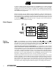
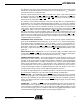
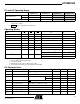
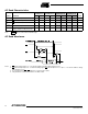
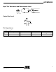
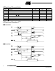
Table Of Contents
- Features
- Description
- Pin Configurations
- Block Diagram
- Device Operation
- Absolute Maximum Ratings*
- DC and AC Operating Range
- Operating Modes
- DC Characteristics
- AC Read Characteristics
- AC Read Waveforms
- Input Test Waveforms and Measurement Level
- Output Test Load
- Pin Capacitance
- AC Byte Load Characteristics
- AC Byte Load Waveforms(1)(2)
- Program Cycle Characteristics
- Software Protected Program Waveform
- Programming Algorithm(1)
- Data Polling Characteristics(1)(2)
- Data Polling Waveforms
- Toggle Bit Characteristics(1)
- Toggle Bit Waveforms(1)(3)
- Software Product Identification Entry(1)
- Software Product Identification Exit(1)
- Boot Block Lockout Feature Enable Algorithm(1)
- Ordering Information
- Packaging Information
10
AT29BV020
0402D–FLASH–05/02
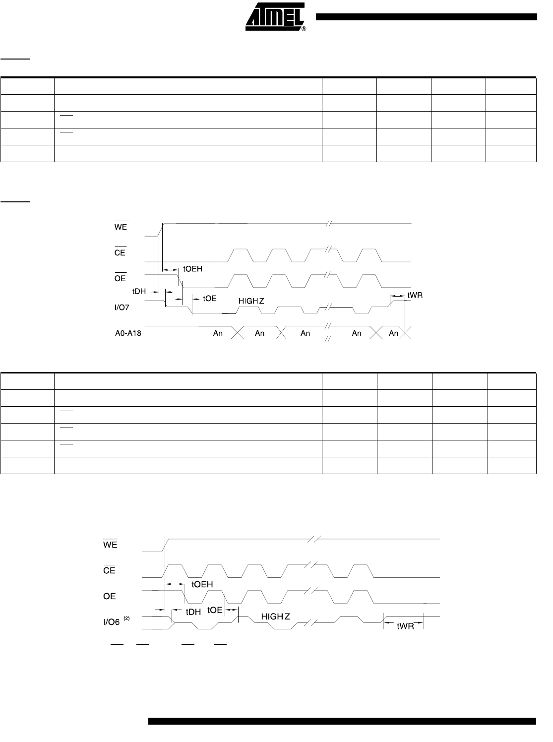
Notes: 1. These parameters are characterized and not 100% tested.
2. See t
OE
spec in AC Read Characteristics.
Data Polling Waveforms
Notes: 1. These parameters are characterized and not 100% tested.
2. See t
OE
spec in AC Read Characteristics.
Toggle Bit Waveforms
(1)(3)
Notes: 1. Toggling either OE or CE or both OE and CE will operate toggle bit.
2. Beginning and ending state of I/O6 will vary.
3. Any address location may be used but the address should not vary.
Data Polling Characteristics
(1)(2)
Symbol Parameter Min Typ Max Units
t
DH
Data Hold Time 10 ns
t
OEH
OE Hold Time 10 ns
t
OE
OE to Output Delay
(2)
ns
t
WR
Write Recovery Time 0 ns
Toggle Bit Characteristics
(1)
Symbol Parameter Min Typ Max Units
t
DH
Data Hold Time 10 ns
t
OEH
OE Hold Time 10 ns
t
OE
OE to Output Delay
(2)
ns
t
OEHP
OE High Pulse 150 ns
t
WR
Write Recovery Time 0 ns