
Manual


5
AT29BV010A
0519D–FLASH–05/02
Note: 1. After power is applied and V
CC
is at the minimum specified data sheet value, the system should wait 20 ms before an oper-
ational mode is started.
Notes: 1. X can be VIL or VIH.
2. Refer to AC Programming Waveforms.
3. VH = 12.0V ± 0.5V.
4. Manufacturer Code is 1F. The Device Code is 35.
5. See details under Software Product Identification Entry/Exit
.
DC and AC Operating Range
AT29BV010A-12 AT29BV010A-15 AT29BV010A-20 AT29BV010A-25 AT29BV010A-30
Operating
Temperature (Case)
Com. 0°C-70°C0°C-70°C
0°C-70°C 0°C-70°C 0°C-70°C
Ind. -40°C-85°C-40°C-85°C
-40°C-85°C -40°C-85°C
V
CC
Power Supply
(1)
2.7V to 3.6V 2.7V to 3.6V 2.7V to 3.6V 2.7V to 3.6V 2.7V to 3.6V
2.
Not recommended for New Designs.
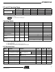
Operating Modes
Mode CE OE WE Ai I/O
Read V
IL
V
IL
V
IH
Ai D
OUT
Program
(2)
V
IL
V
IH
V
IL
Ai D
IN
Standby/Write Inhibit V
IH
X
(1)
XXHighZ
Program Inhibit X X V
IH
Program Inhibit X V
IL
X
Output Disable X V
IH
XHighZ
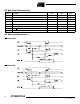
Product Identification
Hardware
V
IL
V
IL
V
IH
A1 - A16 = V
IL
,A9=V
H
(3)
,A0=V
IL
Manufacturer Code
(4)
A1 - A16 = V
IL
,A9=V
H
(3)
,A0=V
IH
Device Code
(4)
Software
(5)
A0 = V
IL,
A1 - A16 = V
IL
Manufacturer Code
(4)
A0 = V
IH,
A1 - A16 = V
IL
Device Code
(4)
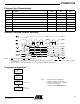
DC Characteristics
Symbol Parameter Condition Min Max Units
I
LO
Output Leakage Current V
I/O
=0VtoV
CC
1µA
I
SB1
V
CC
Standby Current CMOS CE =V
CC
-0.3VtoV
CC
Com. 40 µA
Ind. 50 µA
I
SB2
V
CC
Standby Current TTL CE =2.0VtoV
CC
1mA
I
CC
V
CC
Active Current f = 5 MHz; I
OUT
=0mA;V
CC
=3.6V 15 mA
V
IL
Input Low Voltage 0.6 V
V
IH
Input High Voltage 2.0 V
V
OL
Output Low Voltage I
OL
=1.6mA;V
CC
=3.0V 0.45 V
V
OH
Output High Voltage I
OH
=-100µA;V
CC
=3.0V 2.4 V