
User Manual


AT28C040
2
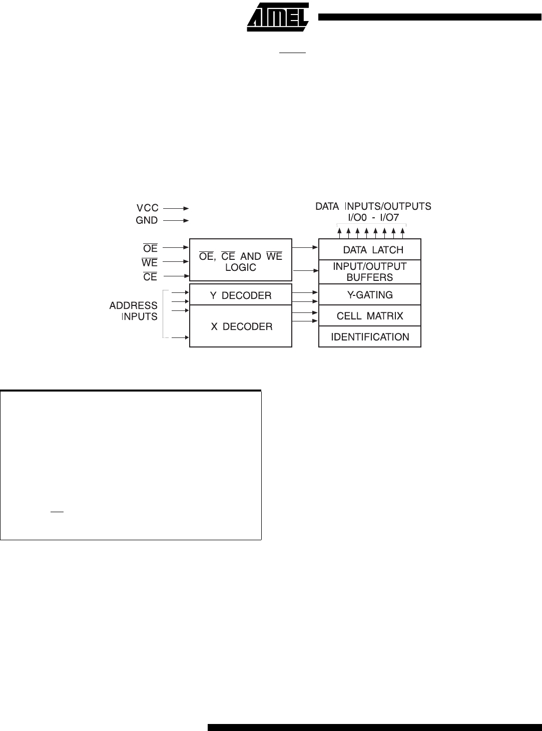
The AT28C040 is accessed like a static RAM for the read
or write cycle without the need for external components.
The devi ce c ontai ns a 256-by te pa ge regi ster to a llow writ-
ing of u p to 256 b yt es simul tan eou sl y. Dur in g a wr it e cyc le ,
the address and 1 to 256 bytes of data are internally
latched, freeing the address and data bus for other opera-
tions. Following the initiation of a write cycle, the device will
automatically write the latched data using an internal con-
trol timer. The end of a write cycle can be detected by
DATA
POLLING of I/O7. Once th e end of a write cy cle has
been detected, a new access for a read or write can begin.
Atmel's AT28C040 has add itional features to ensure high
quality and manufacturability. The device utilizes internal
error correction for extended endurance and improved data
retention characteristics. An optional software data protec-
tion mechanism is available to guard against inadvertent
writes. The device also includes an extra 256 bytes of
EEPROM for device identification or tracking.
Bloc k Diagram
Absolute Maximum Ratings*
Temperature Under Bias................................ -55
°
C to +125
°
C
*NOTICE: Stresses beyond those listed under “Absolute
Maximum Ratings” may cause per manent dam-
age to the device. This is a stres s ra ting onl y and
funct ion al ope ration of th e d evice at these o r any
other conditions beyond those indicated in the
operational sections of this specification is not
implied. Exposure to absolute maximum rating
conditi ons f or e xtended p eriods ma y af fect dev ice
reliability .
Storage Temperature ..................................... -65
°
C to +150
°
C
All Input Voltages
(including NC pins)
with Respect to Ground ...................................-0.6V to +6.25V
All Output Voltages
with Respect to Ground .............................-0.6V to V
CC
+ 0.6V
Voltage on OE
and A9
with Respect to Ground ...................................-0.6V to +13.5V