
Owner's manual

AT27BV020
8
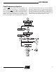
Notes: 1. V
CC
must be applied simultaneously or before V
PP
and removed simultaneously or after V
PP
.
2. This parameter is only sampled and is not 100% tested. Output Float is defined as the point where data is no longer driven
—see timing diagram.
3. Program Pulse width tolerance is 100 µsec ± 5%.
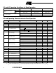
Note: 1. The AT27BV020 has the same Product Identification Code as the AT27C020. Both are programming compatible.
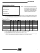
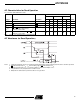
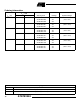
AC Programming Characteristics
T
A
= 25 ± 5°C, V
CC
= 6.5 ± 0.25V, V
PP
= 13.0 ± 0.25V
Symbol Parameter Test Conditions
(1)
Limits
UnitsMin Max
t
AS
Address Setup Time
Input Rise and Fall Times:
(10% to 90%) 20ns
Input Pulse Levels:
0.45V to 2.4V
Input Timing Reference Level:
0.8V to 2.0V
Output Timing Reference Level:
0.8V to 2.0V
2µs
t
CES
CE Setup Time 2 µs
t
OES
OE Setup Time 2 µs
t
DS
Data Setup Time 2 µs
t
AH
Address Hold Time 0 µs
t
DH
Data Hold Time 2 µs
t
DFP
OE High to Output Float Delay
(3)
0 130 ns
t
VPS
V
PP
Setup Time 2 µs
t
VCS
V
CC
Setup Time 2 µs
t
PW
PGM Program Pulse Width
(2)
95 105 µs
t
OE
Data Valid from OE 150 ns
t
PRT
V
PP
Pulse Rise Time During
Programming
50 ns
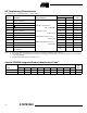
Atmel’s 27BV020 Integrated Product Identification Code
(1)
Codes
Pins
Hex
DataA0 O7 O6 O5 O4 O3 O2 O1 O0
Manufacturer 0000111101E
Device Type 11000011086