
Manual
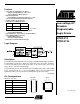
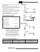
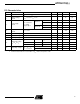
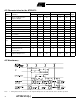
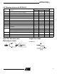
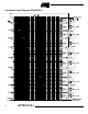
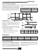
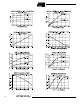
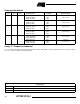
Table Of Contents
- Pin Configurations
- DC and AC Operating Conditions
- Features
- Logic Diagram
- Description
- Absolute Maximum Ratings*
- Logic Options
- Output Options
- DC Characteristics
- AC Characteristics for the AT22LV10
- AC Waveforms(1)
- AC Characteristics for the AT22LV10L
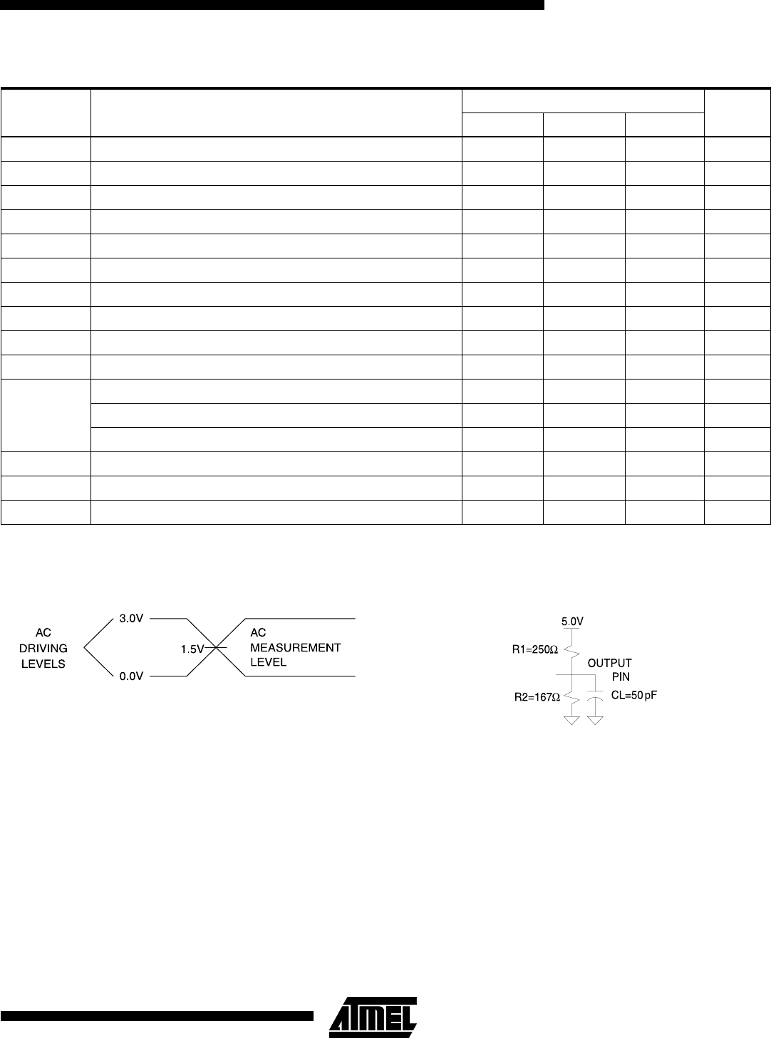
- Input Test Waveforms and Measurement Levels
- Output Test Loads
- Functional Logic Diagram AT22LV10(L)
- Preload of Registered Outputs
- Power-up Reset
- Pin Capacitance
- Erasure Characteristics
- Ordering Information
- Using “C” Product for Industrial
AT22LV10(L)
5
Input Test Waveforms and
Measurement Levels
Output Test Loads
Commercial
AC Characteristics for the AT22LV10L
Symbol Parameter
AT22LV10L-25
UnitsMin Typ Max
t
PD
Input or Feedback to Non-Registered Output 15 25 ns
t
EA
Input to Output Enable 15 25 ns
t
ER
Input to Output Disable 15 25 ns
t
CF
Clock to Feedback 0 5 9 ns
t
CO
Clock to Output 0 10 14 ns
t
SF
Feedback Setup Time 12 7 ns
t
S
Input Setup Time 17 15 ns
t
H
Hold Time 0 ns
t
P
Clock Period 12 ns
t
W
Clock Width 6 ns
F
MAX
External Feedback 1/(t
S
+ t
CO
)32.2MHz
Internal Feedback 1/(t
SF
+ t
CF
)47.6MHz
No Feedback 1/(t
P
) 83.3 MHz
t
AW
Asynchronous Reset Width 25 15 ns
t
AR
Asynchronous Reset Recovery Time 25 15 ns
t
AP
Asynchronous Reset to Registered Output Reset 18 28 ns