
Instruction Manual


Table Of Contents
- Features
- Description
- Pin Configuration
- Block Diagram
- Device Description
- Pin Description
- FPGA Master Serial Mode Summary
- Control of Configuration
- Cascading Serial Configuration Devices
- Programming Mode
- Standby Mode
- Absolute Maximum Ratings*
- Operating Conditions
- DC Characteristics
- AC Characteristics
- AC Characteristics when Cascading
- AC Characteristics
- Thermal Resistance Coefficients(1)
- Ordering Information
- Packaging Information
12
AT17F040/080
3039C–CNFG–11/02
Notes: 1. For more information refer to the “Thermal Characteristics of Atmel’s Packages”, available on the Atmel web site, at
http://www.atmel.com/atmel/acrobat/doc0636.pdf.
2. Airflow = 0 ft/min.
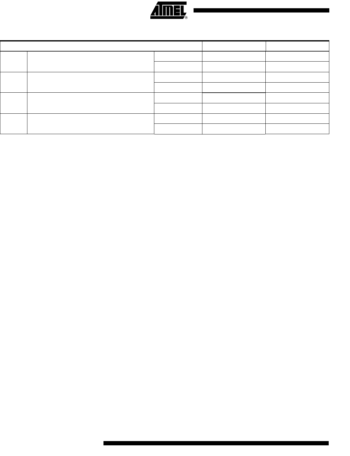
Thermal Resistance Coefficients
(1)
Package Type AT17F040 AT17F080
8CN4 Leadless Array Package (LAP)
q
JC
[°C/W] –
q
JA
[°C/W]
(2)
–
20J Plastic Leaded Chip Carrier (PLCC)
q
JC
[°C/W] –
q
JA
[°C/W]
(2)
–
44A Thin Plastic Quad Flat Package (TQFP)
q
JC
[°C/W] – 17
q
JA
[°C/W]
(2)
–62
44J Plastic Leaded Chip Carrier (PLCC)
q
JC
[°C/W] – 15
q
JA
[°C/W]
(2)
–50