
Owner's manual


Preliminary
APR6016 Data Sheet
Voice Recording & Playback Device Page 17
Revision 1.0
Electrical Characteristics
The followin
g
tables list Absolute Maximum Ratin
g
s, Recom-
mended DC Characteristics, and recommended AC Charac-
teristics for the APR6016 device.
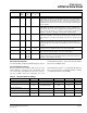
Absolute Maximum Ratings
Stresses
g
reater than those listed in Table 4 ma
y
cause per-
manent dama
g
e to the device. These specifications repre-
sent a stress ratin
g
onl
y
. Operation of the device at these or
an
y
other conditions above those specified in the recom-
mended DC Characteristics or recommended AC Character-
istics of this specification is not implied. Maximum conditions
for extended periods ma
y
affect reliabilit
y
.
Table 4 Absolute Maximum Ratings.
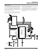
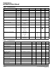
ANAIN+ 17 19
Non-Inverting Analog Input: T
his input is the non-inverting input for the analog
signal that the user wishes to record. When the device is used in a differential
input configuration this pin should receive a 16 mV peak to peak input coupled
through a 0.1 uF capacitor. When the device is used in a single ended input con-
figuration this pin should receive a 32 mV peak to peak input coupled through a
0.1 uF capacitor.
/BUSY 21 23
Busy Output: T
his active low output is low during either a record, playback,
DIG_WRITE, DIG_READ or fast forward operation. The pin is tri-stated other-
wise. This pin can be connected to an LED to indicate playback/record operation
to the user. This pin can also be connected to an external microcontroller as an
indication of the status of playback, record, forward, or digital operation.
VCCD 27 30, 31, 32
Digital Power Supply: T
his connection supplies power for all on-chip digital cir-
cuitry. This pin should be connected to the 3.0 V power plane through a via. This
pin should also be connected to a 0.1 uF bypass cap as close to the pin as possi-
ble.
VCCA 18 20, 21
Analog Power Supply: T
his connection supplies power for all on-chip analog
circuitry. This pin should be connected to the 3.0 V power plane through a via.
This pin should also be connected to a 0.1 uF bypass cap as close to the pin as
possible.
VSSA 12,23 12, 13, 14, 24,
25, 26
Analog Ground:
These pins should be connected to the ground plane through a
via. The connection should be made as close to the pin as possible.
VSSD 4 5, 6
Digital Ground: Th
is pin should be connected to the ground plane through a via.
The connection should be made as close to the pin as possible.
NC 5, 6, 7,
10, 19,
20, 22
1, 7, 8, 22
No Connect:
These pins should not be connected to anything on the board. Con-
nection of these pins to any signal, GND or VCC may result in incorrect device
behavior or cause damage to the device.
Pin Name Pin No.
28 pin
TSOP
Pin No.
28 pin
DIP
Pad No. (Die)
Reference Figure
18
Functionality
Item Symbol Condition Min Max Unit
Power Supply voltage
V
CC
T
A
= 25 C
-0.3 7.0 V
Input Voltage
V
IN
T
A
= 25
C
Device VCC = 3.0 V -0.3 5.5 V
Storage Temperature
T
STG
- -65 150
o
C
Temperature Under Bias
T
BS
- -65 125
o
C
Lead Temperature
T
LD
<10s 300
o
C