
User guide


Voice Recording & Playback Device Page 3
Revision 2.1
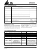
Memory Organization
The APR6008 memory array is organized to allow the great-
est flexibilit
y in message management and digital storage.
The smallest addressable memor
y unit is called a “sector”.
The APR6008 contains 640 sectors.
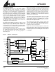
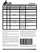
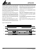
Figure 3 Memory Map.
Sectors 0 through 639 can be used for analog storage. Du -
ring
audio recording one memory cell is used per sample
clock c
ycle. When recording is stopped an end of data (EOD)
bit is programed into the memory. This prevents playback of
silence when partial sectors are used. Unused memor
y that
exists between the EOD bit and the end of the sector can not
be used.
Sectors 0 throu
gh 9 are tested and guaranteed for digital
stora
ge. Other sectors, with the exception of sector 639, can
store data but have not been tested, and are thus not
guaran-
teed to provide 100%
good bits. This can be managed with
error correction or forward check-before-store methods.
Once a write c
ycle is initiated all previously written data in the
chosen sector is lost.
Mixin
g audio signals and digital data within the same sector is
not possible.
Note: There are a total of 15bits reserved for addressing. The
APR6008 only
requires 10 bits. The additional 5 bits are used
for larger devices within the APR6008 family.
SPI Interface
All memory management is handled by an external host pro-
cessor. The host processor communicates with the APR6008
throu
gh a simple Serial Peripheral Interface (SPI) Port. The
SPI port can run on as little as three wires or as man
y as
seven dependin
g on the amount of control necessary. This
section will describe how to mana
ge memory using the
APR6008 SPI Port and associated OpCode commands.
This topic is broken down into the followin
g sections:
•Sendin
g Commands to the Device
•OpCode Command Description
•Receivin
g Device Information
•Current Device Status
(CDS)
•Reading the Silicon Identification (SID)
•Writin
g Digital Data
•Readin
g Digital Data
•Recordin
g Audio Data
•Pla
ying Back Audio Data
•Handshakin
g Signals
Sending Commands to the Device
This section describes the process of sendin
g OpCodes to
the APR6008 All Opcodes are sent in the same wa
y with the
exception of the
DIG_WRITE
and
DIG_READ
commands
.
The
DIG_WRITE and DIG_READ
commands
are
described
in the
Writing Digital Data
and
Reading Digital Data
sections
that follow. The minimum SPI confi
guration needed to send
commands uses the DI, /CS, and SCLK pins. The device will
accept inputs on the DI pin whenever the /CS pin is low.
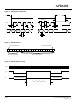
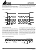
OpCode commands are clocked in on the risin
g edge of the
SPI clock. Fi
gure 4 shows the timing diagram for shifting
OpCode commands into the device. Figure 5 is a description
of the OpCode stream.
You must wait for a command to finish executin
g before send-
in
g a new command. This is accomplished by monitoring the /
BUSY pin. You can substitute monitorin
g of the busy pin by
inserting a fixed delay between commands. The required
dela
y is specified as
T
next1
,T
next2
,T
next3
or T
next4
. Figure 6
shows the timin
g diagram for sending consecutive com-
mands. Table 1 describes which
T
next
specification to use.
Sector 0
Sector 1
Sector 639
Can Not be Used for Digital Data
SAC Trigger Point
APR6008